Advanced Packaging Semiconductor Market Overview
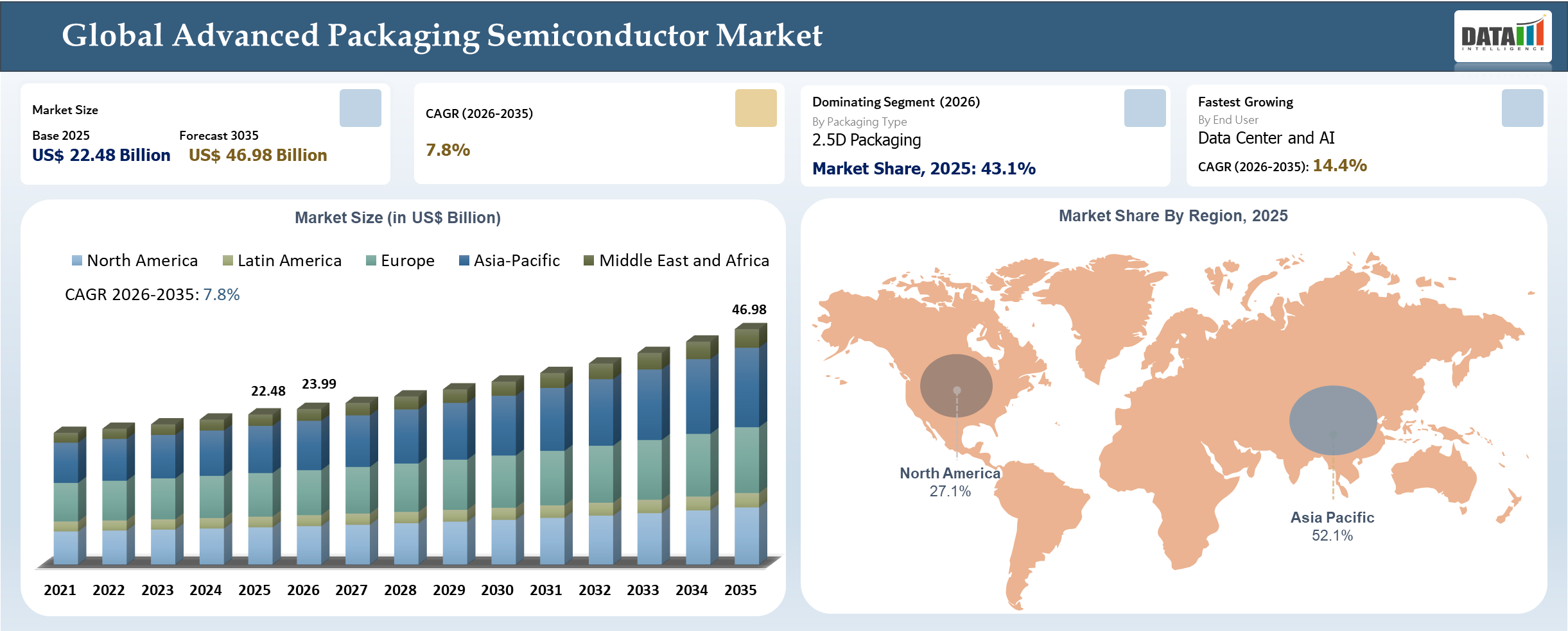
The global advanced packaging semiconductor market reached US$ 22.48 billion in 2025 and is expected to reach US$ 46.98 billion by 2035, growing with a CAGR of 7.8% during the forecast period 2026-2035. Investments driven by policy have become more influential for advanced semiconductor packaging, as policymakers have realized that advanced packaging acts as a major bottleneck for semiconductor manufacturing operations. Investments made under the U.S. CHIPS and Science Act, like the National Advanced Packaging Manufacturing Program (NAPMP), have provided significant amounts of capital to invest in R&D and pilot line facilities to promote advanced packaging capacity in the country. Similar efforts in Asia, particularly in India and China, involve the establishment of local ecosystems to decrease dependence on traditional hotspots and increase capacity in advanced packaging.
Advanced Packaging Semiconductor Industry Trends and Strategic Insights
- Advanced packaging technology is integrated into semiconductor design to achieve logic-memory integration for AI and HPC applications with companies like Taiwan Semiconductor Manufacturing Company Limited synchronizing their packaging technology with their products' development.
- The industry is evolving into a market with chiplet architecture and heterogenous integration, which allows for more flexibility in mixing several dies into one package. It helps in reducing dependence on the shrinking of nodes, while increasing yield and efficiency. Organizations such as Intel Corporation and Samsung Electronics Co., Ltd. are investing heavily in packaging technologies.
- Packaging technology continues to be heavily concentrated in terms of capacity among a few select suppliers, causing supply shortages, especially for 2.5D and 3D solutions. High customer demand in AI and data centers has resulted in an emphasis on serving high-end customers, thus giving top companies like ASE Technology Holding Co., Ltd. and Amkor Technology, Inc. a competitive advantage through price negotiation and contracting.
Market Scope
| Metrics | Details | |
| 2025 Market Size | US$ 22.48 Billion | |
| 2035 Projected Market Size | US$ 46.98 Billion | |
| CAGR (2026-2035) | 7.8% | |
| Largest Market | Asia-Pacific | |
| Fastest Growing Market | North America | |
| By Packaging Type | 2.5D Packaging, 3D Packaging, Fan Out Packaging, Wafer Level Packaging and System in Package | |
| By Interconnect | TSV, Hybrid Bonding, Bump and Copper Pillar and RDL | |
| By Device Type | Logic and Processor, Memory, RF and Connectivity, Power Devices and Sensor and MEMS | |
| By End User | Data Center and AI, Consumer Electronics, Automotive, Telecom and Industrial | |
| By OSAT and Foundry Type | Foundry Integrated, OSAT Led and IDM Led | |
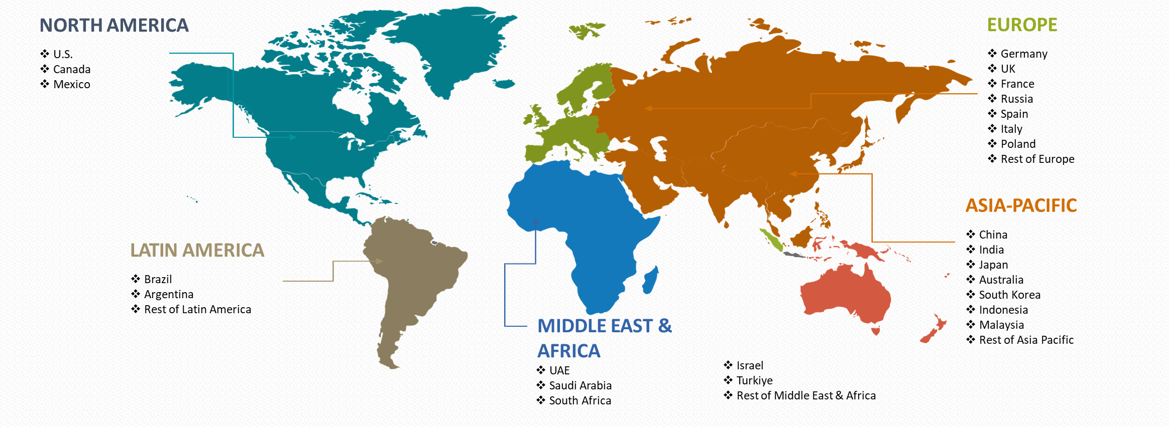
| By Region | North America | U.S., Canada, Mexico |
| Europe | Germany, UK, France, Spain, Italy, Poland | |
| Asia-Pacific | China, India, Japan, Australia, South Korea, Indonesia, Malaysia | |
| Latin America | Brazil, Argentina | |
| Middle East and Africa | UAE, Saudi Arabia, South Africa, Israel, Turkiye | |
| Report Insights Covered | Competitive Landscape Analysis, Company Profile Analysis, Market Size, Share, Growth | |
AI Impact Analysis
AI is causing an impact on the advanced semiconductor packaging market due to its focus on high-performance applications. The demand is being focused towards AI accelerators and data center processors, which are using an integrated circuit design that incorporates logic chips and high bandwidth memory, resulting in a disproportionate usage of advanced semiconductor packaging technology, such as 2.5D interposer and 3D chip-stacking. Consequently, this is causing the allocation of capacity towards select high value projects that are being executed by companies like NVIDIA Corporation.
The concentration of demand is causing changes in the revenue allocation and pricing within the industry. The packaging firms have shifted their focus toward long-term agreements with the hyperscalers and AI chipmakers where they can forecast their volumes, and the margin is high. On the other hand, the smaller or non-AI players will suffer from longer lead times and restricted availability to advanced nodes.
The emergence of AI is also leading to shifts in technology road maps and capital allocation towards packaging technologies that can help integrate memory and enable high interconnect density. Leading chip manufacturers like Samsung Electronics Co., Ltd., and SK hynix Inc. are developing their packaging technologies with an emphasis on HBM and AI-oriented architecture, highlighting the reliance of future semiconductor capabilities on advanced packaging technologies. The synergy between AI and packaging is fueling market specialization.
Disruption Analysis
Advanced Packaging Redefines Semiconductor Value Chain Through Architecture Shift and Capacity Constraints
The main disruptor in the advanced semiconductor packaging industry lies in the transition from the architectural approach of monolithic scaling to the approaches of chiplets and heterogenous integration. With the limitations in terms of economics and technology in scaling nodes, there has been a change in system architecture designs that involve distributing functionality among several dies, which are then integrated in the package itself. Advanced packaging has now become more of a design decision than a fabrication decision. Leading players like Intel Corporation and Taiwan Semiconductor Manufacturing Company Limited have started incorporating packaging within their product architectures.
Additionally, disruptions are occurring in terms of capacity concentration and bottlenecks in advanced packaging supply chains. Advanced packaging technologies including 2.5D and 3D ICs rely on restricted substrate sources, proprietary equipment, and high-yield production capabilities that are currently available with only a small number of suppliers. It leads to structural limitations in that supply cannot instantly meet demand, especially due to the rising demand for these products in AI and data centers. Consequently, there has been an increase in investments in regional capacity growth and vertical integration within the industry.
BCG Matrix: Company Evaluation
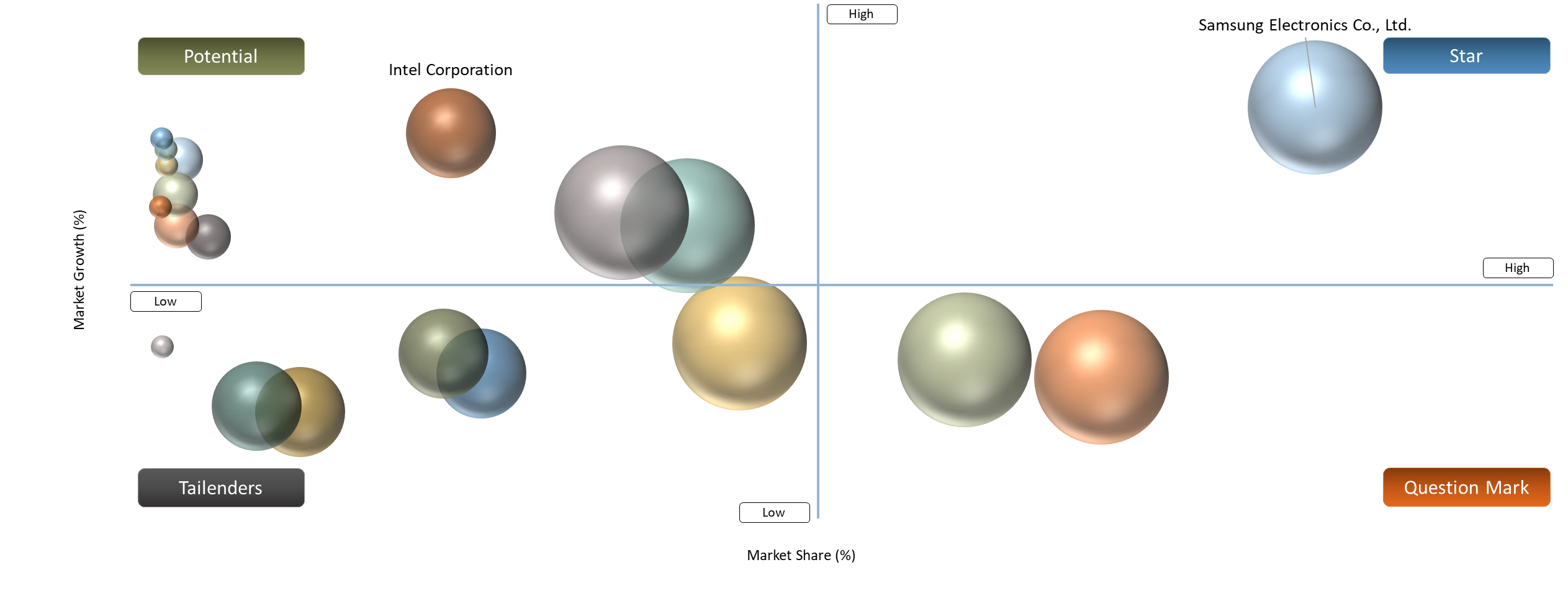
The advanced semiconductor packaging industry is dominated by Star firms such as Taiwan Semiconductor Manufacturing Company Limited, Samsung Electronics Co., Ltd., and Intel Corporation, whose business model is characterized by market penetration and exposure to growth. This business model is supported by their integrated capabilities in design, fabrication, and advanced packaging, especially for AI, high-performance computing, and chiplets. position is sustained through consistent development of 2.5D and 3D packaging technologies and alignment with the requirements of hyperscalers, leading to premium value creation and technology roadmap shaping.
Question Mark companies like Amkor Technology, Inc., JCET Group Co., Ltd., and Tongfu Microelectronics Co., Ltd. have been ramping up their advanced packaging capacity but are still at a transitional stage, weighing their opportunities against risks of implementation. On the other hand, Cash Flow and Stable firms such as ASE Technology Holding Co., Ltd., Powertech Technology Inc., and Siliconware Precision Industries Co., Ltd. continue to hold their ground with their economies of scale, customer base, and consistent demand in conventional and advanced packaging offerings.
The "Tailenders" group consists of firms that have low differentiation capabilities when it comes to advanced packaging or are less integrated into the market, like IBM Corporation, Cadence Design Systems, Inc., and Applied Materials, Inc., and therefore operate within the market through their role as part of the ecosystem rather than from their capabilities in terms of advanced packaging.
Market Dynamics
Rising Demand for High Bandwidth and Power Efficiency Accelerates Adoption of 2.5D and 3D Packaging
The growing challenges with bandwidth capacity, energy efficiency, and size of components are making advanced packaging solutions such as 2.5D, 3D, and Hybrid Bonding more prevalent. With the rising complexity of AI and high-performance computing loads, current packaging solutions cannot provide sufficient speed and cooling capabilities. Advanced packaging allows for closer interconnectivity between logic and memory components and thus greatly enhances both the bandwidth capacity and energy efficiency.
The trend can be seen in the deployment strategies of industries, where firms like SK hynix Inc. and Micron Technology, Inc. are adopting high-bandwidth memory technology through 3D stacking, and Taiwan Semiconductor Manufacturing Company Limited is using interposer-based 2.5D architectures to cater to the rising demands of AI. With the increasing demands of systems beyond conventional packaging techniques, this technology plays a pivotal role in supporting advancements in performance, making it an integral part of future growth in the market.
Long qualification cycles and yield sensitivity, combined with the concentration of advanced packaging capacity
The longer qualification period and sensitivity to yields, together with the consolidation of advanced packaging manufacturing capabilities, constitute the greater constraint on the industry. The advanced packaging solutions that incorporate 2.5D and 3D integration need to go through rigorous qualification for designs, materials, and fabrication processes prior to commercial launch. The process takes considerable time and is very sensitive to yield issues, where small imperfections may greatly affect costs and scalability.
Restraint is further reinforced by the availability of only a few players capable of offering advanced packaging solutions, such as Taiwan Semiconductor Manufacturing Company Limited and ASE Technology Holding Co., Ltd.. Capacity shortages lead to limited availability of supply, especially at times when there is a great deal of demand for products used in AI and high-performance computing. Throughput becomes constrained and time taken to fulfill orders is increased, preventing the industry from scaling efficiently.
Segmentation Analysis
The global advanced packaging semiconductor market is segmented based on packaging type, interconnect, device type, end user, OSAT and foundry type and region.
2.5D Packaging Drives Volume Adoption While 3D Packaging Enables Next-Generation Performance Scaling
The market for next-generation semiconductor packaging is dominated by 2.5D packaging because of its high compatibility with existing semiconductor architecture and eco-systems. It is used extensively in AI accelerators and supercomputers, where companies like Taiwan Semiconductor Manufacturing Company Limited have relied on interposers to package logic and memory with great efficacy. Its usage continues to be popular due to its feasibility in manufacturing, well-established supply chain, and stable cost-to-performance ratio, which allows large-scale adoption in leading semiconductor initiatives.
3D packaging is growing at a rapid pace, especially in areas that require higher density performance and system integration. Some of the companies involved in developing new solutions in this field include Samsung Electronics Co., Ltd. and SK hynix Inc. These companies have been focusing on vertical stacking and hybrid bonding technologies that can enable memory-heavy applications like AI and data centers.
Geographical Penetration
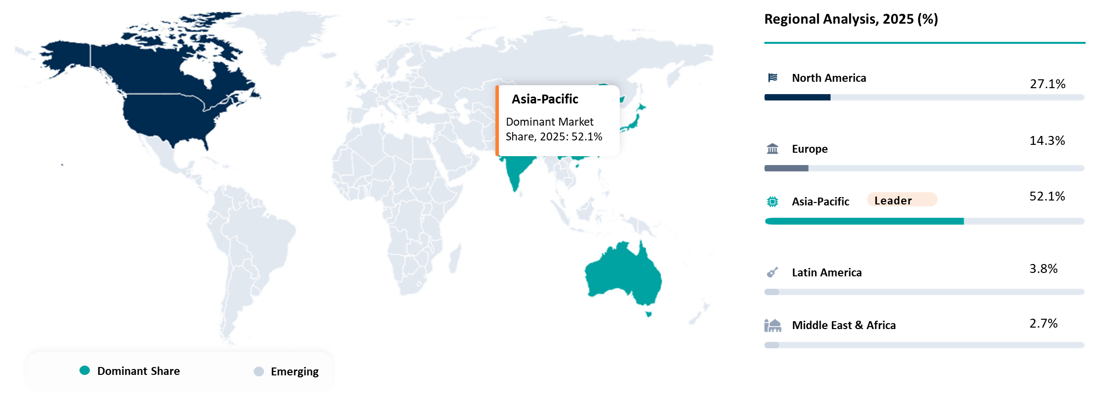
Asia-Pacific Advanced Semiconductor Packaging Market: Capacity Dominance Driven by AI, Policy Push, and Supply Chain Clustering
Asia-Pacific continues to be a hub of the execution of advanced semiconductor packaging technology due to extensive integration between foundries, outsourced assembly and test providers (OSAT), and memory makers. The Asia-Pacific region accounts for the largest number of facilities for semiconductor packaging globally, with major players like Taiwan Semiconductor Manufacturing Company (TSMC), Samsung, and Advanced Semiconductor Engineering, Inc. (ASE) continually increasing their capacity to address growing demands from artificial intelligence (AI) and high-performance computing.
The current policy landscape of Asian countries in the region is focused on increasing the resilience of their supply chains and strengthening their local capabilities. Countries like China, Japan, South Korea, and India are adopting industrial policies that allow the localization of semiconductor fabrication processes to decrease their dependence on foreign entities. The People's Republic of China has allocated more than $140 billion worth of semiconductor subsidies, whereas other nations are encouraging packaging, research and development, and training programs.
Regional disparities are also reinforced by investments and manufacturing trends. Taiwan and South Korea control the niche market of high-end packaging associated with advanced nodes and memory, while Southeast Asia – Malaysia, Vietnam, and Singapore – is positioning itself as a relatively inexpensive back-end center thanks to the diversification of the global supply chain. Specifically, Malaysia intends to raise its share of semiconductors in GDP and expand packaging capabilities, whereas China is pouring money into internal packaging facilities.
Taiwan: Global Nucleus of Advanced Packaging and AI Chip Integration
Taiwan dominates the advanced packaging industry owing to the semiconductor ecosystem it has established, with TSMC being the key company that dominates the leading-edge chip fabrication and advanced packaging sectors. The technology known as CoWoS (chip on wafer on substrate) is crucial in the manufacture of AI chips, and most global companies rely on Taiwan for the provision of highly efficient packaging options.
High levels of investment are being observed, with the expansion of cutting-edge packaging plants to meet the demands created by artificial intelligence. In Taiwan, the favorable trade dynamics include excellent supply chain networks, access to a skilled labor force, and proximity to important clients, which ensures that the utilization levels are very high along with technological superiority. It is also crucial for exportation of advanced chips.
China: Policy-Driven Expansion and Catch-Up Strategy in Advanced Packaging
The Chinese advanced packaging industry features substantial government-funded and driven growth of manufacturing capacity to reduce China’s dependence on other countries’ semiconductor technology. The Chinese government has launched several funding schemes worth billions of dollars to develop and build up the capability of indigenous companies like JCET and Tongfu Microelectronics.
The investments in China’s semiconductor packaging industry are focused on creating complete ecosystems within the country, ranging from materials to substrates and test facilities. Advanced packaging solutions are being adopted by firms to cater to needs related to artificial intelligence, 5G, and automobiles. Furthermore, the role of China in international business is shifting from a cheap assembly player to that of a leading provider of advanced packaging solutions.
Competitive Landscape
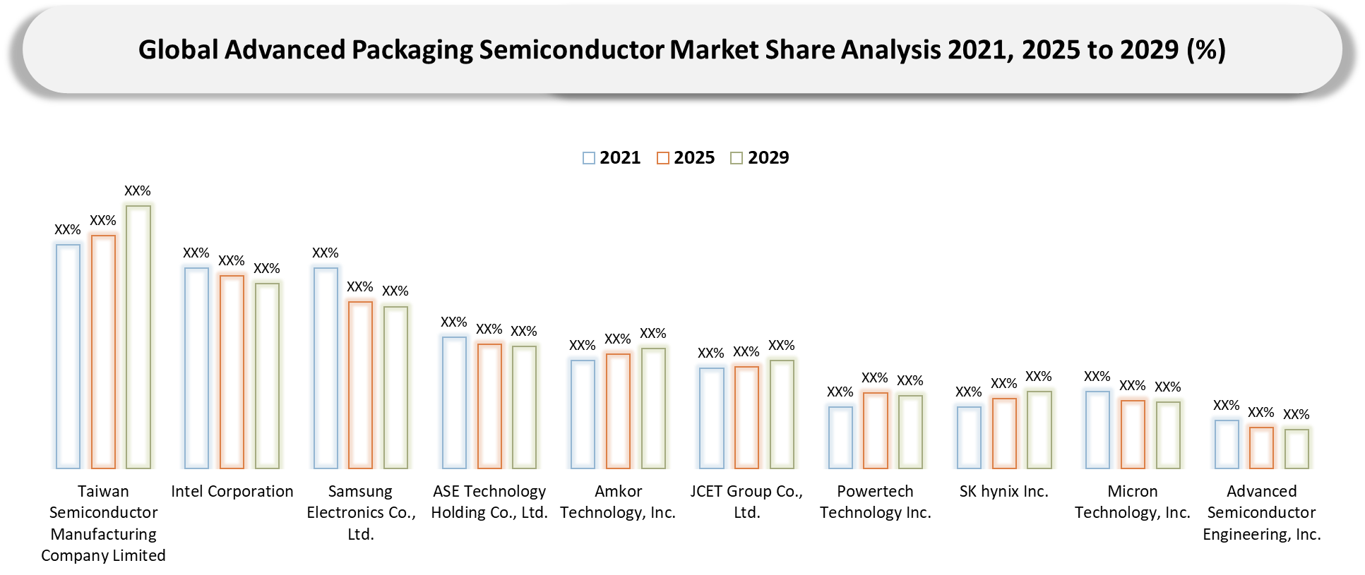
The market for advanced semiconductor packaging technologies includes integrated firms like Taiwan Semiconductor Manufacturing Company Limited, Samsung Electronics Co., Ltd., and Intel Corporation, which have great expertise in 2.5D/3D packaging and chiplet-based design solutions. Other key suppliers in this industry include ASE Technology Holding Co., Ltd., Amkor Technology, Inc., and JCET Group Co., Ltd., which facilitate high-volume production for AI and HPC-related applications.
- Memory producers SK hynix Inc. and Micron Technology, Inc., along with the equipment suppliers Applied Materials, Inc. and BESI, drive competition as they facilitate technological innovations through their processes. The key strategic approach continues to be capacity augmentation, partnership building, and technological innovation to meet increasing demand from artificial intelligence and supercomputers.
Key Developments
- April 2026 - India made a major milestone in the high-end semiconductor packaging industry through the groundbreaking of India’s first 3D heterogeneous integration (3DHI) packaging plant in Odisha. Spearheaded by 3D Glass Solutions, the initiative will set up a greenfield ATMP facility based on glass substrates for high-density packaging of AI, HPC, telecom, and defense sectors, which will go into commercial operations by 2028.
- April 2026 - Resonac Corporation has established an R&D center at Silicon Valley in accordance with US-JOINT, aiming at advancing the development of innovative semiconductor packaging technology. This venture will help in fostering a cooperative working environment with industry partners, and also in reducing development time, thus facilitating quicker commercialization of advanced packaging technology.
- January 2026 - FPT has invested in building a cutting-edge semiconductor testing and packaging factory in Vietnam, thereby increasing Vietnam’s capability in backend manufacturing. The factory will feature multiple testing lines and aims to grow its capabilities in advanced packaging technologies, including Chip Scale Packaging (CSP) and Wafer Level Packaging. The initiative boosts Vietnam’s participation in the international semiconductor supply chain and supports local ecosystem development in the testing and packaging sectors.
- October 2025 - The Amkor Technology company announced its plans to build an investment worth US$ 7 billion in a facility in Arizona specializing in packaging and testing. This facility is aimed at increasing the capacity of high-volume semiconductor packaging in the United States.
- September 2025 - LCY Chemical Corp. has unveiled its portfolio of advanced formulations that can be used in the semiconductor advanced packaging industry. This solution revolves around the use of materials that will make the processing procedures more accurate, thus improving process yield and reliability. It is particularly beneficial in AI, high-performance computing, and high-speed communications applications.
- November 2024 - Under the company’s EPIC program, Applied Materials created an innovative approach to collaborating with its ecosystem partners to hasten the commercialization process of new semiconductor packaging technologies. This new collaboration approach focuses on developing high-performance, energy-efficient packaging technologies for artificial intelligence-based computing.
Why Choose DataM?
- Technological Innovations: Explores advancements in advanced semiconductor packaging technologies, including 2.5D/3D integration, chiplet architectures, fan-out wafer-level packaging (FOWLP), hybrid bonding, and glass substrate innovations, which are enhancing performance, power efficiency, and interconnect density for AI and high-performance computing applications.
- Product Performance & Market Positioning: Evaluates how leading players differentiate through packaging density, bandwidth performance, thermal management, yield optimization, and scalability, highlighting competitive positioning across AI processors, memory (HBM), and advanced logic devices.
- Real-World Evidence: Highlights deployment of advanced packaging in data centers, AI accelerators, high-performance computing systems, 5G infrastructure, and automotive electronics, demonstrating improvements in system performance, miniaturization, and energy efficiency.
- Market Updates & Industry Changes: Tracks developments such as capacity expansions in advanced packaging facilities, R&D investments, government incentives (e.g., CHIPS Act), emergence of new packaging materials, and increasing adoption of heterogeneous integration across regions including Asia Pacific and North America.
- Competitive Strategies: Analyzes how key companies expand through technology partnerships, ecosystem collaborations, OSAT capacity expansion, vertical integration (foundry + packaging), and innovation in chiplet and 3D packaging platforms.
- Pricing & Market Access: Explains pricing dynamics based on packaging complexity (2.5D vs 3D), wafer-level vs substrate-based solutions, and integration requirements, along with access strategies through OSAT partnerships, foundry services, and long-term supply agreements with fabless semiconductor firms.
- Market Entry & Expansion: Identifies growth opportunities driven by AI, HPC, and advanced memory demand, with expansion strategies focused on regional diversification of packaging capacity, government-supported semiconductor initiatives, and development of end-to-end semiconductor ecosystems.
Target Audience 2026
- Integrated Device Manufacturers (IDMs) and Foundries: Semiconductor companies integrating advanced packaging technologies such as 2.5D/3D and chiplet architectures to enhance performance, yield, and system-level integration.
- OSAT Providers (Outsourced Semiconductor Assembly and Test): Service providers expanding capabilities in advanced packaging, wafer-level packaging, and heterogeneous integration to meet rising demand from AI, HPC, and memory applications.
- Fabless Semiconductor Companies: Design firms relying on advanced packaging solutions to enable high-performance processors, AI accelerators, and custom silicon, particularly for data center and edge applications.
- Cloud Service Providers and Hyperscalers: Organizations driving demand for advanced packaging-enabled chips to support AI workloads, high-performance computing, and large-scale data center infrastructure.
- Memory Manufacturers: Companies developing HBM and advanced memory solutions that depend on 3D stacking and advanced packaging technologies for bandwidth and performance optimization.
- Equipment and Material Suppliers: Providers of substrates, bonding technologies, deposition equipment, and specialty materials critical for enabling advanced packaging processes and scalability.
- Investors & Private Equity Firms: Entities investing in advanced packaging infrastructure, OSAT expansion, and next-generation semiconductor technologies driven by AI and digital transformation demand.
- Dealers & Distribution Networks: Authorized distributors, service providers and aftermarket suppliers involved in sales, financing, spare parts and maintenance services.