Graphene Based Silicon Photonics Market Overview
Graphene Moves From Lab Material To Foundry Relevant Photonics Layer
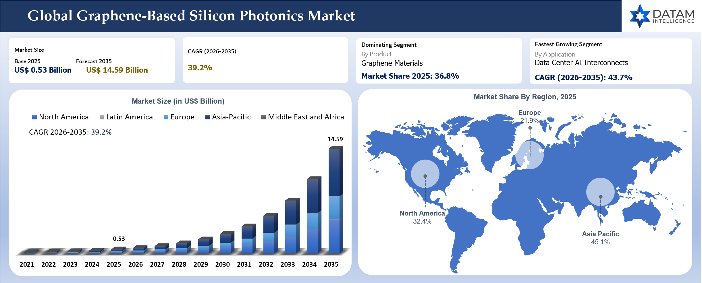
The global graphene based silicon photonics market reached US$ 0.53 billion in 2025 and is expected to reach US$ 14.59 billion by 2035 growing at a CAGR of 39.4% during 2026 to 2035. Graphene photonics is moving from a research led field toward a foundry relevant platform because electrical interconnects and conventional optical device materials are under pressure from AI infrastructure, data center power limits and demand for higher bandwidth density. Graphene offers a thin, broadband and electrically tunable material layer that can support modulation, detection and sensing functions without replacing the entire silicon process stack. Commercial interest is strongest where existing photonic systems face power, footprint, heat or wavelength flexibility constraints.
Commercial maturity remains uneven. Graphene wafers and graphene sensing devices are already available from specialized suppliers while graphene photonic chips for datacom and AI interconnects remain closer to pilot commercialization. The strongest near term revenue pools are therefore linked to graphene materials, device prototyping, MPW access, process integration, design enablement and reliability services. Finished photonic products will scale later as foundry repeatability and packaging readiness improve.
AI infrastructure creates the largest strategic pull because rack scale and package scale data movement is becoming a material bottleneck. NVIDIA now promotes CPO switches with integrated silicon photonics for AI networking and claims 5x better power efficiency over pluggable transceivers. Graphene based approaches are not yet competing at the same commercial scale, but the direction of travel is clear: optical links are being pulled closer to ASICs, switch silicon and accelerator packages.
Key Takeaways
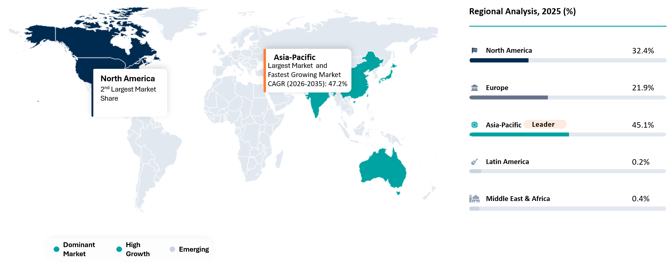
- Asia-Pacific dominated the market with 45.1% share in 2025 supported by semiconductor manufacturing, photonics research, advanced packaging activity and sensor development across China, Japan, South Korea, Singapore and Malaysia.
- North America remained a high-value market in 2025 with 32.4% share because AI hardware companies, fabless photonics developers, hyperscale data center ecosystems and advanced semiconductor programs are actively evaluating lower power optical interconnect technologies.
- Europe held 21.9% share in 2025 supported by graphene photonics activity in Germany and Italy, graphene materials and sensing companies in Spain and UK and strong research infrastructure across integrated photonics and advanced materials.
- Asia-Pacific is expected to remain the fastest-scaling region through 2035 as semiconductor foundries, optical component suppliers, packaging providers and AI hardware ecosystems increase focus on photonic integration and wafer level manufacturability.
- Products remain central to market value creation as graphene photonic chips, graphene sensing chips and graphene materials and wafer products move from research prototypes toward pilot production, custom device fabrication and early commercial validation.
- Services are becoming a critical monetization route because graphene integration services, MPW and shuttle programs, PDK and design enablement and qualification support help bridge the gap between lab performance and manufacturable device platforms.
- Data center AI interconnects are expected to remain a major demand driver as optical connectivity moves closer to compute infrastructure and suppliers focus on lower power, higher bandwidth and denser chip communication architectures.
- Medical and biosensing, industrial gas and chemical sensing and quantum and cryogenic systems are creating early specialized demand where graphene’s sensitivity, compact device structure and material properties can support high-value use cases before large-scale AI interconnect adoption matures.
Market Scope
| Metrics | Details | |
| 2025 Market Size | US$ 0.53 Billion | |
| 2035 Projected Market Size | US$ 14.59 Billion | |
| CAGR (2026-2035) | 39.4% | |
| Largest Market | Asia-Pacific, 45.1% Share in 2025 | |
| Fastest Growing Market | Asia-Pacific | |
| Dominating Product | Graphene Materials and Wafer Products, 36.8% Share in 2025 | |
| Fastest Growing Application | Data Center AI Interconnects, CAGR of 43.7% Between 2026 and 2035 | |
| By Offering | Products, Services | |
| By Distribution Channel | Direct Device Product Sales, Direct Wafer and Material Sales, Direct Foundry Sales, MPW and Shuttle Programs, Joint Development Programs, PDK and Design Ecosystem Access | |
| By Manufacturing Platform | 150 mm and Below Wafer Platform, 200 mm Wafer Platform, 300 mm Wafer Platform, Others | |
| By Application | Data Center AI Interconnects, Telecom Optical Transport, Medical and Biosensing, Industrial Gas and Chemical Sensing, Quantum and Cryogenic Systems, Automotive LiDAR and Imaging, Research and Prototyping, Others | |
| By End-User | Fabless Photonics Companies, Optical Module Vendors, AI Hardware Companies, Telecom Equipment Vendors, Sensor Companies, Medical Device Companies, Industrial OEMs, Automotive OEM and Tier 1, Research Institutes, Government Funded Programs, Others | |
| By Region | North America | U.S., Canada, Mexico |
| Europe | Germany, UK, France, Spain, Italy, Poland | |
| Asia-Pacific | China, India, Japan, Australia, South Korea, Indonesia, Malaysia | |
| Latin America | Brazil, Argentina | |
| Middle East and Africa | UAE, Saudi Arabia, South Africa, Israel, Turkiye | |
| Report Insights Covered | Competitive Landscape Analysis, Company Profile Analysis, Market Size, Share, Growth | |
Why This Report Matters in 2026
2026 marks an important inflection point for the graphene based silicon photonics market because the technology is moving beyond academic validation and into foundry linked commercialization. AI infrastructure is increasing pressure on data movement power limits while photonic integration is shifting closer to chips, packages and wafer level manufacturing. A market that was previously viewed as experimental is now being shaped by pilot lines, MPW access, graphene device portfolios and early foundry service models.
Graphene based photonic chips and sensing platforms are becoming more relevant as buyers look for lower power optical links, compact sensing devices and manufacturable material platforms. Black Semiconductor’s FabONE activity, Graphenea’s GFAB services, Paragraf’s graphene device portfolio and NVIDIA’s silicon photonics CPO push show how the wider ecosystem is moving toward practical device integration. 2026 is therefore a critical year to understand which revenue pools are real, which applications remain early and which service models can convert prototype activity into commercial demand.
Procurement, partnership and investment decisions in 2026 need stronger evidence around wafer scale repeatability, graphene transfer yield, BEOL compatibility, packaging readiness and customer qualification timelines. Report coverage matters because early winners will not be decided only by device performance. Commercial advantage will come from companies that can connect material quality, foundry process access, device validation and ecosystem partnerships into a credible path toward scalable production.
Strategic Indicators for Graphene-Based Silicon Photonics
Industry Trends and Strategic Insights
Commercialization Is Shifting Toward Wafer Access, Device Repeatability and Packaging Readiness
Wafer scale integration is becoming the main gating factor. Academic performance claims matter less to buyers than stable transfer, clean patterning, contact reliability, low defect density and repeatable optical response across wafers. Graphene offers foundry services on custom wafers up to 6 inch and Paragraf has promoted graphene device manufacturing progress on 6 inch wafers. Black Semiconductor is building a 300 mm pilot line path through FabONE. Commercial success will depend on whether device performance can survive process scaling.
Graphene photonic chips are being pulled by two different demand clusters. AI interconnect demand is focused on high speed, low power chip communication. Sensing demand is focused on high sensitivity, fast response, small footprint and operation in harsh or specialized environments. The first cluster requires tight integration with semiconductor packaging and optical I O architectures. The second cluster can monetize earlier through lower output high value applications in biosensing, molecular sensing, gas detection and cryogenic measurement.
Design enablement is becoming a commercial product in its own right. AIM Photonics emphasizes PDKs, MPW, fabrication, validation and packaging as part of the integrated photonics development cycle. Graphene platforms will need similar design rules, material models, reliability data and packaging guidelines before fabless developers can design with confidence. Companies that control the process module and design environment will have a stronger position than companies selling only graphene films.
Signals That Matter Before Large Scale Revenue Arrives
Foundry readiness is the most important leading indicator. Active indicators include MPW availability, wafer size expansion, PDK release, test vehicle publication, process control documentation and early customer qualification. Black Semiconductor’s FabONE plan, AIM Photonics’ assembly design kit activity and Graphenea’s GFAB service point toward a market where prototyping access is as important as end product demand.
Customer readiness is the second signal. Fabless photonics companies, sensor developers, AI hardware firms and telecom equipment vendors will not move from evaluation to commercial engagement without credible reliability evidence. Graphene sensing products appear closer to customer adoption because Paragraf already sells sensor product ranges and highlights molecular sensing, cryogenic, quantum computing and automotive applications. Photonic interconnect chips need more proof around insertion loss, driver integration, photodetector stability, packaging and thermal behavior.
Ecosystem partnerships matter because no single company can commercialize the stack alone. Graphene material suppliers, photonic designers, foundries, packaging firms, EDA vendors and end system developers must align around a usable process flow. The strategic opportunity is therefore not limited to device sales. Revenue can come from wafers, custom device fabrication, MPW runs, process modules, PDK access, testing, packaging and qualification programs.
High Regulation Impact
Regulatory impact is high because graphene photonic and sensing products sit at the intersection of semiconductor manufacturing, export controls, telecom qualification, medical validation and environmental material handling. Devices used in data center or telecom infrastructure must pass customer reliability programs and may be affected by semiconductor export rules. Medical and molecular sensing devices face more formal validation pathways when used in diagnostics. Foundry services also require strong quality systems, traceability, material handling documentation and customer data protection. Companies with ISO certified processes, controlled cleanroom flows and clear product documentation will have a practical advantage.
High Investment Activity
Investment activity is high but concentrated. Funding is flowing toward chip connectivity, semiconductor sovereignty, advanced packaging and photonics manufacturing access. Black Semiconductor’s disclosed financing and FabONE buildout show how capital intensive graphene photonics becomes once companies move from prototypes toward wafer scale production. Public private infrastructure such as AIM Photonics also shows institutional support for photonic manufacturing, packaging and workforce development. Capital is less available for vague graphene claims and more available for platforms tied to AI interconnects, semiconductor process flows, sensing use cases and manufacturable device programs.
Supply Chain Disruption
Supply chain risk is concentrated around graphene quality, wafer availability, transfer process yield, cleanroom compatibility and packaging access. Graphene materials can vary by growth method, transfer method, substrate and contamination level. Photonic device performance is highly sensitive to small process deviations, which makes supplier qualification more demanding than ordinary material purchasing. Packaging creates another risk point because optical coupling, electronic integration and test infrastructure remain specialized. A disruption in graphene films, wafer level processing, metallization or photonic packaging can delay customer qualification even when device design is ready.
Pricing Volatility
Pricing volatility is most visible in custom wafers, GFET chips, foundry runs, MPW participation and qualification services. Graphenea’s official store shows openly priced products such as GFET chips, graphene on substrates and GFAB services, which signals a real but still specialized commercial supply base. Larger photonic chip programs are usually quoted through custom projects, so pricing can move with wafer size, mask count, process complexity, transfer yield and test requirements. Early buyers should expect project based pricing rather than standardized component pricing until process modules become more mature.
Procurement Pressure
Procurement pressure is rising because buyers need proof before committing to graphene device programs. Purchasing teams will ask for wafer level uniformity, process control data, reliability reports, packaging compatibility, supplier continuity and clear ownership of design rules. Cost alone will not decide vendor selection. Procurement teams will favor suppliers that reduce program risk through test vehicles, MPW access, FA support and transparent qualification plans. Suppliers without strong documentation may struggle even if device performance looks attractive in lab results.
New Technology Adoption
Adoption will be staged. Research institutes and fabless developers will adopt first through prototype chips, MPW runs and custom wafers. Sensor companies will follow where graphene sensing performance can solve specific biosensing, gas sensing or cryogenic measurement problems. Telecom and AI infrastructure adoption will take longer because reliability, packaging and qualification barriers are higher. The strongest adoption pathway is likely a service led model where customers first buy process access, test vehicles and qualification work before committing to product integration.
Recent Merger and Acquisition or Funding
- April 2026: Paragraf and Archer Materials announced a strategic collaboration on graphene based quantum devices extending graphene device activity into quantum and cryogenic use cases
- March 2025: NVIDIA expanded its silicon photonics CPO ecosystem through partner enabled fabrication packaging laser and optical fiber supply chains involving TSMC SPIL Lumentum Sumitomo Coherent Corning Senko Foxconn and Fabrinet
- February 2025: Black Semiconductor moved into FabONE in Aachen Germany and advanced its 300 mm wafer pilot line roadmap for graphene based optical chip technology
- June 2024: Black Semiconductor secured EUR 254.4 million in funding to launch graphene photonic technology including EUR 228.7 million in public funding and EUR 25.7 million in equity funding
New Product Launches
- May 2026: Paragraf introduced PMF2000 GFET activity through its official product updates, expanding its graphene electronic device portfolio for advanced sensing and device development
- August 2025: NVIDIA introduced Quantum X InfiniBand Photonics and Spectrum X Photonics CPO systems for AI factories, including 115 Tb per second Quantum X switching capacity and Spectrum X Photonics systems scaling up to 409.6 Tb per second
- March 2025: NVIDIA launched silicon photonics based network switching systems at GTC 2025, integrating silicon photonics directly with NVIDIA Quantum and NVIDIA Spectrum switch ICs to reduce power consumption, latency and component complexity in AI data centers
- 2025: Graphenea listed mGFET 4D for sensing applications, GFET S20 for sensing applications and GFAB Graphene Foundry Services through its official product store, supporting device prototyping and custom graphene device fabrication
- 2025: 2D Photonics advanced its graphene integrated photonics platform for energy saving optical interconnects, wavelength independent operation across O band, C band and L band and future optical transceiver applications
Regional Expansion Opportunity
Regional expansion should focus on countries with strong semiconductor or photonics ecosystems. U.S. demand is anchored by AI infrastructure, optical I O research and photonics prototyping. Germany and Italy are relevant because direct graphene photonics activity is visible through Black Semiconductor and 2D Photonics. UK has a strong graphene sensor base through Paragraf. Japan offers a disciplined route for photonics, sensing and semiconductor qualification. Singapore, South Korea and Malaysia offer process, packaging and foundry ecosystems that can support early commercialization.
Government Policy Support
Policy support is strongest where graphene photonics overlaps with semiconductor sovereignty, photonics manufacturing and advanced packaging. AIM Photonics is one of the U.S. manufacturing innovation institutes and provides public private infrastructure for integrated photonics development. Europe’s semiconductor policy direction supports pilot lines, advanced materials and strategic chip capacity even though direct graphene photonics funding remains selective. Public funding is likely to favor projects with measurable links to AI infrastructure, energy efficient computing, quantum systems, healthcare sensing or domestic semiconductor capability.
AI Impact Analysis
Optical Interconnect Pressure Is Pulling New Materials Into The Compute Stack
AI training and inference infrastructure is forcing a rethink of data movement. Compute density is increasing faster than electrical links can efficiently support across packages, boards and racks. NVIDIA’s silicon photonics page frames CPO switches as a way to replace pluggable transceivers with optics on the same package as the ASIC. The same structural pressure creates room for graphene because broadband optical response and compact electro optical behavior can help reduce link energy and footprint in future architectures.
Graphene will not become an AI hardware material simply because AI demand is rising. Buyers will require evidence that graphene devices can be manufactured, packaged and qualified at semiconductor relevant reliability levels. A promising modulator or photodetector architecture must translate into testable chips, repeatable process modules and compatible packaging flows. AI increases urgency, but manufacturability determines adoption.
AI also changes the route to market. Traditional photonics commercialization often moved from research prototypes into telecom modules. AI hardware may pull graphene devices through co development programs, chiplet packaging projects and optical I O pilot platforms instead. Market participants with MPW services and PDK support could become more important than standalone device vendors during the early commercialization phase.
Disruption Analysis
Graphene Challenges Device Assumptions Rather Than The Entire Photonics Stack
Graphene’s disruptive potential sits at the device layer. Conventional silicon photonics relies on silicon waveguides, germanium photodetectors, III V lasers, silicon modulators and complex packaging methods. Graphene does not replace every layer. It can modify specific functions where broadband operation, electrical tunability, compact device geometry and low energy operation create a commercial edge.
The most immediate disruption is likely in modulators and photodetectors. Graphene can support broadband optical interaction across multiple wavelength bands and can be integrated as an atomically thin active layer. 2D Photonics highlights wavelength independent operation across O, C and L bands for graphene integrated photonics. Such flexibility is relevant because future systems may need broader wavelength use, higher WDM density and simplified device design.
Sensing is a second disruption area because graphene responds strongly to surface interactions. Paragraf’s graphene molecular sensors target nucleic acids, proteins, gas, ions, small molecules, environmental sensing, food and beverage, agriculture and healthcare use cases. Photonics based sensing could benefit where optical readout, miniaturization and sensitivity need to work together. Market disruption will occur gradually through high value pilot use cases rather than a sudden replacement of incumbent sensor platforms.
BCG Matrix: Company Evaluation
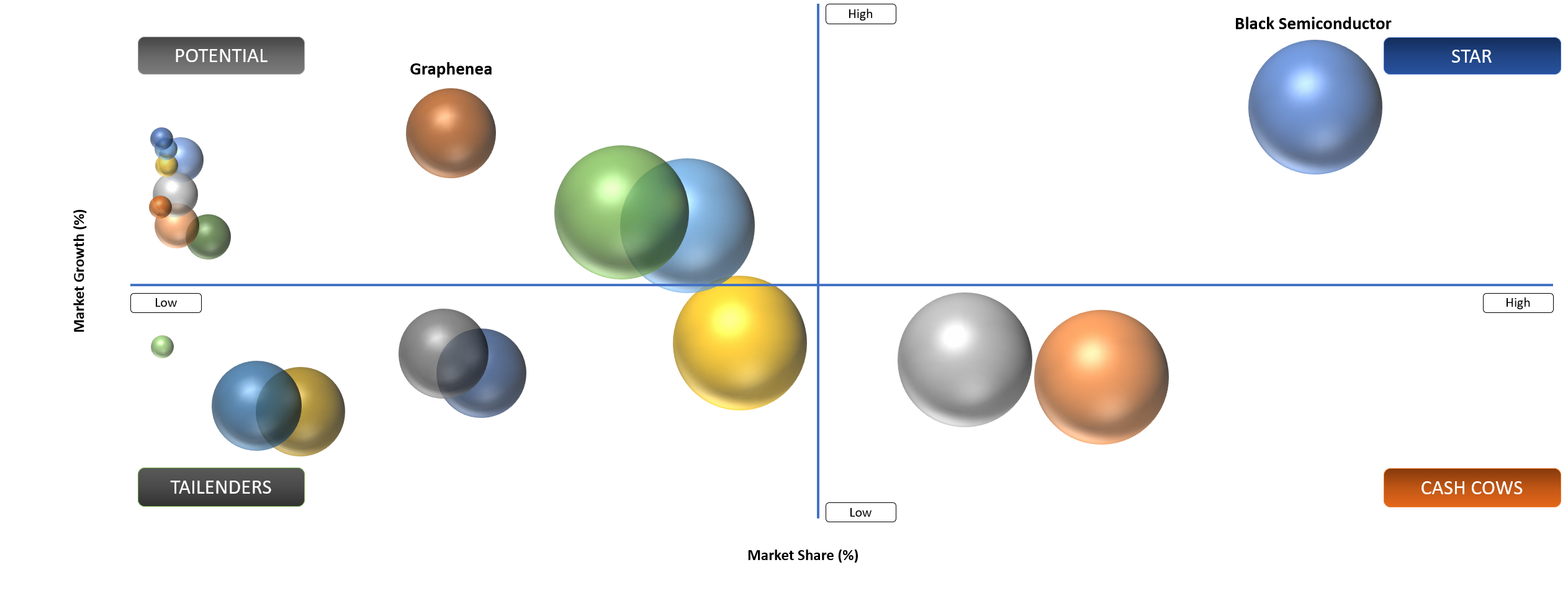
STAR
Black Semiconductor and 2D Photonics are the most relevant Stars in the direct graphene photonics landscape because both are positioned around graphene enabled photonic connectivity rather than general graphene supply. Black Semiconductor has a clear chip connectivity narrative, BEOL compatibility language, a 300 mm pilot line ambition and large funding disclosure. 2D Photonics has a direct datacom and telecom orientation with positioning around energy efficient transceiver solutions, high bandwidth density and compatibility with foundry tools. Both companies are still scaling, but their strategic fit with optical interconnect demand is stronger than general graphene material suppliers.
Potential
Graphenea and Paragraf sit in the Potential category because both already sell active graphene products or services that can support commercialization but their direct exposure to photonic interconnect chips is less central. Graphenea brings GFET chips, CVD films and custom foundry services that can support prototyping and device development. Paragraf brings graphene molecular sensors, Hall sensors and custom 2D foundry services with visible use cases in healthcare, environmental sensing, cryogenics, quantum computing and automotive systems. Both companies can influence the market if their material and sensor platforms connect more deeply with photonic integration needs.
Market Dynamics
Driver Impact Analysis
| Driver | Market Growth Impact | Demand Concentration | Impacted Use Case | Strategic Impact |
Wafer scale graphene integration moves photonic chips closer to foundry commercialization | High | Germany, U.S., Italy and Malaysia | Graphene photonic chips and graphene optical interconnect chips | Supports transition from lab prototypes to wafer level process revenue |
AI interconnect power limits increase demand for lower energy optical links | High | U.S., Japan and South Korea | Data center AI interconnects and optical I O | Strengthens long term demand for graphene modulator and photodetector validation |
MPW access reduces prototype cost for graphene photonic device developers | Medium To High | U.S., Europe, Singapore and Malaysia | Research prototyping, MPW runs and PDK design enablement | Creates earlier revenue through shared wafer runs and customer test vehicles |
AI Interconnect Power Limits
AI infrastructure is forcing optical connectivity closer to compute. Rack scale accelerators, high bandwidth memory, switch ASICs and chiplet packages require data movement that is faster, cooler and more energy efficient than conventional electrical interconnects. NVIDIA’s CPO messaging around million GPU AI factories shows how power efficiency and resiliency have moved from engineering concerns to buying criteria. Graphene photonic devices become relevant because they target low power modulation, detection and compact optical integration.
Commercial demand is not limited to hyperscale operators. Fabless photonics developers, custom accelerator companies, optical module vendors and packaging ecosystems need new device options that can support future optical I O roadmaps. Graphene offers a material route for high speed electro optical functions without requiring a full replacement of existing silicon photonics infrastructure.
The driver is strongest where graphene can solve measurable pain points: lower drive voltage, wider wavelength operation, smaller device footprint, reduced thermal load or easier integration into existing CMOS linked flows. Commercial success will depend on the ability to convert those advantages into qualified devices and repeatable foundry recipes.
Restraint Impact Analysis
| Restraint | Drag On Market Growth | Primary Impact Area | Impacted Use Case | Strategic Impact |
Graphene transfer yield limits repeatability across wafer scale production | High | Foundry integration and device fabrication | Graphene modulator chips and graphene photodetector chips | Slows customer qualification until process control data improves |
Customer qualification delays slow conversion from prototype to commercial orders | Medium To High | Telecom, AI infrastructure and medical sensing | Optical interconnects, biosensing chips and industrial sensing chips | Extends sales cycles and increases need for reliability testing and validation support |
Graphene Transfer Yield
Graphene integration remains difficult because performance depends on material quality, transfer cleanliness, contact resistance, dielectric compatibility and process repeatability. A device that works on a lab sample may not perform consistently across wafer lots. Buyers in photonics and semiconductor manufacturing will expect process control, test data and reliability evidence before committing to commercial designs.
Packaging creates another restraint. Photonic devices require fiber coupling, electrical drive, thermal control, optical alignment and reliable assembly. AIM Photonics’ focus on test, assembly and packaging highlights how packaging can become a bottleneck even when chip fabrication is technically feasible. Graphene adds more process variables and increases the need for qualification data.
The restraint is not permanent, but it slows conversion from prototype demand to repeatable revenue. Stronger metrology, stable wafer supply, MPW access and design enablement can reduce risk. Companies that package graphene processes as reliable manufacturing modules will be better positioned than those selling raw material performance alone.
Segmentation Analysis
Graphene Photonic Chips Become The First High Value Test For Commercial Readiness
Graphene photonic chips represent the most important commercial test for the market because they connect material innovation with high value demand in optical interconnects. The category includes graphene modulator chips, graphene photodetector chips and graphene optical interconnect chips. Each device type targets a specific weakness in existing architectures: modulation energy, receiver footprint, broadband operation or chip to chip communication density.
Graphene modulator chips are especially important because modulation is one of the core functions in optical data movement. Black Semiconductor describes graphene as enabling compact, low power and high speed integration of photonics and electronics at the chip level. 2D Photonics also positions graphene integrated photonics around high bandwidth density, low power consumption and optical transceiver solutions. Commercial interest will rise where these claims become supported by foundry data, stable PDK models and packaging ready prototypes.
Graphene photodetector chips matter because receiver energy and footprint are critical in large scale optical systems. Graphene can enable compact detection architectures and has research support for broadband operation. Commercial deployment will depend on dark current control, responsivity, contact stability, thermal performance and integration with TIAs or receiver electronics.
Graphene optical interconnect chips sit one step closer to system architecture. Black Semiconductor’s chip connectivity positioning is relevant because optical chip communication is becoming a strategic issue for AI computing. Such products will require deeper co design with chiplet packaging, EICs, optical coupling and system validation. Early revenue may appear through co development programs before standardized products are widely available.
Graphene Modulator Chips
Graphene modulator chips target one of the most valuable functions in photonic systems: converting electrical signals into optical signals at high speed with low energy use. Conventional modulators can face tradeoffs between speed, size, insertion loss, temperature sensitivity and drive voltage. Graphene’s atomically thin structure and electro optical response create interest in compact broadband modulation.
Commercial traction will depend on manufacturable device geometry. Buyers will look for repeatable insertion loss, extinction ratio, bandwidth, driver compatibility and thermal stability. Strong claims around performance need to be converted into wafer level control metrics. MPW access can help customers compare graphene devices against silicon microring or Mach Zehnder alternatives using the same evaluation structure.
Graphene modulator chips are most relevant to AI interconnects and telecom optical transport. AI infrastructure rewards low power and high density. Telecom rewards wavelength flexibility and stable operation across O, C and L bands. 2D Photonics’ emphasis on wavelength independent operation across these bands gives a useful commercial signal.
Graphene Photodetector Chips
Graphene photodetector chips address receiver side constraints in optical systems. Conventional receivers often require germanium integration, careful contact engineering and additional amplification. Graphene based photodetectors can create interest because they may support broadband detection and compact integration. Commercial value will depend on whether responsivity, noise, bandwidth and reliability meet buyer requirements.
Graphene photodetectors will likely commercialize first in specialized use cases before becoming mainstream in AI interconnects. Research and prototyping applications can tolerate lower standardization if the device offers unique measurement capability. Telecom and data center buyers will require stronger qualification and supply assurance.
A useful commercial path is to combine graphene photodetector test vehicles with foundry services, wafer products and qualification support. Device companies can then evaluate performance without building a full process flow internally. Such packaging of device development and service revenue fits the current state of the market better than expecting immediate large scale chip sales.
Segmentation
- By Offering
- Products
- Graphene Photonic Chips
- Graphene Sensing Chips
- Graphene Materials And Wafer Products
- Others
- Services
- Graphene Integration Services
- Foundry And MPW Services
- Design And Qualification Services
- Others
- Products
- By Distribution Channel
- Direct Device Product Sales
- Direct Wafer And Material Sales
- Direct Foundry Sales
- MPW And Shuttle Programs
- Joint Development Programs
- PDK And Design Ecosystem Access
- By Manufacturing Platform
- 150 mm and Below Wafer Platform
- 200 mm Wafer Platform
- 300 mm Wafer Platform
- Others
- By Application
- Data Center AI Interconnects
- Telecom Optical Transport
- Medical And Biosensing
- Industrial Gas And Chemical Sensing
- Quantum And Cryogenic Systems
- Automotive LiDAR And Imaging
- Research And Prototyping
- Others
- By End-User
- Fabless Photonics Companies
- Optical Module Vendors
- AI Hardware Companies
- Telecom Equipment Vendors
- Sensor Companies
- Medical Device Companies
- Industrial OEMs
- Automotive OEM And Tier 1
- Research Institutes
- Government Funded Programs
- Others
Geographical Penetration
North America Graphene-Based Silicon Photonics Market Trends
North America is strategically important because the U.S. hosts the strongest concentration of AI infrastructure demand, hyperscale cloud spending, fabless silicon design and photonics ecosystem activity. Demand is not driven only by network traffic. It is increasingly shaped by rack level power constraints, chiplet interconnect bottlenecks and advanced packaging requirements. Optical I O and CPO activity from NVIDIA, Intel ecosystem partners and photonics startups creates a strong pull for new active materials.
The U.S. ecosystem also supports prototyping through public private infrastructure. AIM Photonics provides access to design, simulation, fabrication, packaging, validation and a route toward volume manufacturing for integrated photonics users. Such infrastructure is critical for graphene based platforms because early customers need lower cost evaluation paths before committing to process specific designs.
Procurement behavior in North America is likely to favor companies that can prove manufacturing repeatability and packaging readiness. Graphene device suppliers will need more than material performance claims. Stronger adoption will come from PDK availability, MPW schedules, test vehicles, reliability reports and co development programs with AI hardware, telecom and sensing customers.
U.S. Graphene-Based Silicon Photonics Market Landscape
The U.S. is the most important country for early demand because AI hardware, optical networking, chiplet packaging and hyperscale infrastructure are closely connected. NVIDIA’s CPO portfolio highlights how power efficiency, lower latency and serviceability have become design priorities for large AI networks. Graphene photonics can enter this environment where device level power reduction or broadband operation supports future optical I O needs.
U.S. customers are likely to evaluate graphene photonic chips through pilot programs rather than immediate large scale procurement. Fabless photonics companies and AI hardware developers will need MPW access, design support and packaging partnerships. Graphene materials alone will not be enough. Commercial success will require full development support from wafer to tested device.
The country also offers a strong route for sensing applications. Paragraf’s graphene sensing portfolio reflects a broader international interest in graphene devices across molecular sensing, cryogenics, quantum computing and automotive systems. Medical, industrial and quantum sensing customers in the U.S. may offer earlier monetization than large scale AI interconnect chips because project values can remain high even at early production stages.
Asia-Pacific Graphene-Based Silicon Photonics Market Outlook
Asia-Pacific is important because semiconductor manufacturing, optical component supply chains and advanced packaging capacity are deeply embedded across Japan, South Korea, Singapore, China and Taiwan. Graphene photonics requires process equipment, wafer handling, packaging and testing ecosystems that already exist across the region. The region’s strength is therefore execution capacity rather than only end demand.
Japan, South Korea and Singapore are particularly relevant for early partnerships. Japan has deep optical component, sensor and semiconductor process expertise. South Korea has memory, advanced packaging and AI hardware exposure. Singapore has a strong foundry and photonics ecosystem with links to silicon photonics research and manufacturing.
Graphene based platforms may enter Asia Pacific through sensing, materials, wafer services and co development programs before mass photonic interconnect deployment. Commercial traction will depend on local qualification practices, access to packaging partners and willingness of device makers to adopt nonstandard active materials.
Japan Graphene-Based Silicon Photonics Market Demand
Japan is an attractive country for graphene photonic and sensing development because it combines optical component expertise, precision manufacturing and long term semiconductor policy support. Demand is likely to be selective but technically demanding. Buyers will prioritize reliability, documentation, supply assurance and repeatability.
Telecom optical transport, medical diagnostics, industrial sensing and quantum research create practical pathways for graphene devices. Japan’s established electronics and photonics base allows graphene device developers to work with partners that understand optical packaging and quality systems. Early adoption may start through research institutes, equipment makers and specialized device firms.
Japanese procurement cycles can be slower than startup led markets, but qualification discipline can improve commercial credibility. Successful qualification in Japan would provide a strong reference point for broader Asia Pacific adoption. Graphene photodetectors, graphene sensing chips and reliability services look especially relevant.
Competitive Landscape
Direct Graphene Photonics Players Remain Few While Adjacent Foundries Control Commercial Access
The competitive landscape is still forming. Direct graphene photonics companies are limited, which makes the market different from mature semiconductor categories. Black Semiconductor and 2D Photonics are the clearest direct players focused on graphene photonics for chip connectivity and optical interconnect applications. Both are positioned around power efficient data movement rather than broad graphene material sales.
Graphenea, Paragraf, Graphensic, Grolltex and other graphene material or device companies form the second competitive layer. They do not all compete directly in photonic chips, but they influence supply through graphene films, wafers, GFETs, sensing devices and custom fabrication. Its relevance increases when customers need material quality, wafer formats or specialized graphene process support.
Foundries and photonics infrastructure providers form the third layer. GlobalFoundries and AIM Photonics validate how silicon photonics customers buy access through PDKs, MPW, fabrication, packaging and validation. Silterra, Tower Semiconductor, X FAB and similar foundries may participate where customer projects require compatible process modules. Competition will depend less on headline device performance and more on ability to deliver repeatable wafers, test data and customer support.
Key Developments
- May 2026: Paragraf introduced PMF2000 GFET through its official news updates expanding its graphene electronic device portfolio for advanced sensing and device development
- April 2026: Paragraf and Archer Materials announced a strategic collaboration on graphene based quantum devices supporting commercialization activity around graphene enabled quantum and cryogenic applications
- December 2025: Paragraf produced its first 6 inch graphene wafer at its Huntingdon facility supporting scale up of graphene electronic device manufacturing
- August 2025: NVIDIA introduced Quantum X InfiniBand Photonics and Spectrum X Photonics CPO systems targeting commercial availability in 2026 and supporting large scale AI factory networking
- August 2025: UCIe Consortium released the UCIe 3.0 specification with 64 GT per second performance and enhanced manageability strengthening open chiplet interconnect standards relevant to optical I O and advanced package connectivity
- March 2025: NVIDIA launched silicon photonics based network switching at GTC 2025 combining co packaged silicon photonics with NVIDIA Quantum and NVIDIA Spectrum switch ICs for AI data center networking
- February 2025: Black Semiconductor moved into FabONE in Aachen Germany and announced plans to start construction of a scalable 300 mm wafer pilot line for graphene based optical chip technology during 2025
Key Companies
- Black Semiconductor GmbH
- 2D Photonics SpA
- Graphenea Inc.
- Paragraf Limited
- SilTerra Malaysia Sdn. Bhd.
- Graphensic AB
- Grolltex Inc
- ACS Material LLC
- Levidian Nanosystems Limited
- Advanced Graphene Products S.A.
- Directa Plus S.p.A.
- Versarien plc
- GlobalFoundries Inc.
- LIGENTEC SA
- SMART Photonics B.V.
- X-FAB Silicon Foundries SE
- Tower Semiconductor Ltd.
- Intel Corporation
- Cisco Systems, Inc.
- NVIDIA Corporation
Black Semiconductor GmbH
Black Semiconductor GmbH is the strongest direct company reference for graphene photonic chip connectivity. The company positions its technology around integrating high speed graphene photonics directly onto electronic chips to overcome electrical communication limits. Its messaging is tied to AI scale compute, lower heat, energy efficient chip fabrics and CMOS compatible processing. Such positioning gives the company a sharper commercial narrative than general graphene material suppliers.
Black Semiconductor’s move into FabONE and planned 300 mm pilot line are important because graphene photonics needs wafer scale credibility. A pilot line path makes the company more relevant to semiconductor customers that require reproducible processes and future manufacturability. The company’s disclosed funding also suggests investor and public sector confidence in the long term importance of chip level optical communication.
Its main USP is the combination of graphene material capability, photonic chip connectivity focus and mass production ambition. The company is not only selling graphene as a material. It is building a compute connectivity platform where graphene becomes the active layer for faster chip communication. That strategic direction aligns closely with AI infrastructure pressure and the broader shift toward optical I O.
What DataM Uniquely Provides
DataM connects manufacturer evidence with market sizing logic. Instead of treating graphene as a broad material story, the research separates active commercial offerings from speculative use cases. Graphene photonic chips, sensing chips, materials, wafers, integration services, MPW access, PDK enablement and qualification services are evaluated based on what companies actually sell or actively develop.
DataM also builds a TAM SAM SOM bridge that avoids overstating the opportunity. The broad opportunity can include graphene enabled photonics across AI, telecom, sensing and research. The serviceable opportunity is narrowed to product and service categories with visible supplier activity. The obtainable opportunity is linked to realistic commercialization routes such as MPW, custom foundry services, 200 mm process integration and qualification programs.
DataM’s research approach gives buyers a clearer view of what can be commercialized now and what still needs technical validation. The output is useful for strategy teams, foundries, investors, material suppliers and device companies because it shows where revenue can appear first rather than only describing long term potential.
Major Pain Points
- Wafer level graphene transfer still needs stronger repeatability before large customer programs can scale.
- Material quality varies across suppliers, substrates and deposition methods.
- Photonic device performance depends on contact engineering, dielectric compatibility and clean patterning.
- Packaging readiness remains a bottleneck because optical, electrical and thermal requirements must be managed together.
- PDK availability is limited for graphene specific photonic designs.
- Reliability data is not yet mature enough for many telecom and AI infrastructure customers.
- Graphene photonic products often require custom development rather than catalog based buying.
- Procurement teams struggle to compare graphene based devices with mature silicon or germanium alternatives.
- Direct manufacturer base remains small, which increases supplier concentration risk.
- Commercial pricing is difficult to benchmark because many projects are quoted as custom programs.
Analyst View And Opinion
DMI expects graphene based photonic commercialization to progress through services before large scale product revenue. Foundry access, MPW runs, design enablement and qualification services are likely to create near term revenue while photonic interconnect chips move through pilot validation. The structure is common in emerging semiconductor platforms where design confidence must be built before standardized devices can scale.
DMI expects sensing to remain an important early monetization route. Graphene molecular sensors, Hall sensors, gas sensing and cryogenic sensing have clearer immediate use cases than AI optical interconnect chips. High value specialized applications can tolerate smaller production quantities and longer technical support cycles.
DMI expects AI interconnect demand to shape long term investor interest. Optical I O and CPO roadmaps are creating a clearer commercial need for compact, low power and broadband active photonic devices. Graphene’s position will depend on whether suppliers can demonstrate process repeatability, packaging fit and cost discipline within semiconductor manufacturing environments.
Target Audience
| Target Audience | Why The Report Is Relevant |
| Foundries | Helps evaluate graphene integration, MPW revenue and process module opportunities |
| Fabless Photonics Companies | Supports technology scouting and foundry partner selection |
| Graphene Material Suppliers | Shows where wafers, films and custom materials can convert into device revenue |
| Optical Module Vendors | Identifies future device technologies that may affect transceiver roadmaps |
| AI Hardware Companies | Helps track optical I O materials and chip connectivity alternatives |
| Telecom Equipment Vendors | Supports evaluation of broadband photonic device options |
| Sensor Companies | Highlights biosensing, gas sensing and cryogenic sensing commercialization paths |
| Medical Device Companies | Supports early assessment of graphene sensing platforms |
| Industrial OEMs | Identifies applications in chemical, gas and process monitoring |
| Investors | Helps separate credible commercialization routes from speculative graphene use cases |