Chiplet Testing Market Size and Overview
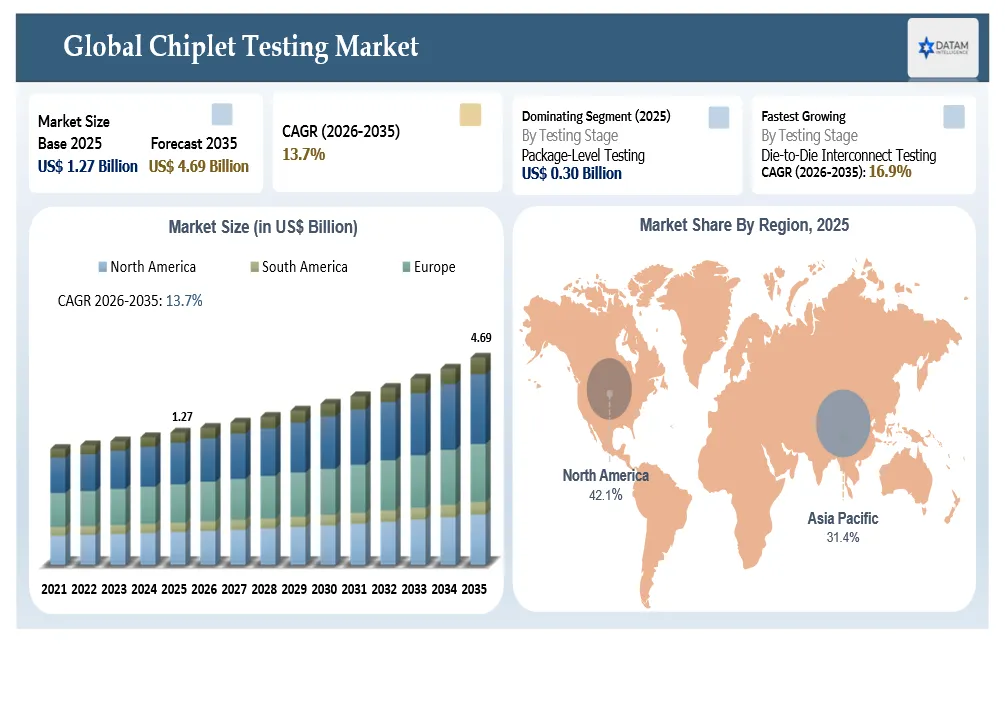
The global Chiplet Testing market reached US$ 1.27 billion in 2025 and is expected to reach US$ 4.69 billion by 2035, growing with a CAGR of 13.7% during the forecast period 2026-2035.
The market is witnessing robust growth as chiplet-based architectures become the preferred design approach for artificial intelligence (AI), high-performance computing (HPC), data center, automotive and networking semiconductors. According to the World Semiconductor Trade Statistics (WSTS), the worldwide semiconductor business revenue for 2025 is estimated to be US$ 795.6 billion, along with the accelerated spending on advanced packaging & heterogeneous integration solutions.2.5D ICs, 3D ICs, FOWLP, Hybrid bonding, HBM, etc., are causing increased challenges and complexity in semiconductor testing; thus, there has been a rise in KGD testing, die-to-die connectivity validation, Package-level and system-level testing. Therefore, manufacturers have been investing heavily in Automated Test Equipment, Probing equipment and artificial intelligence-powered visual inspection machines.
Moreover, the market gets an additional boost through heavy investments in semiconductor fab, packaging technologies and outsourced semiconductor assembly and test (OSAT) facilities located in North America, Taiwan, South Korea, Japan, Europe, as well as new manufacturing centers like India. According to Semiconductor Equipment and Materials International (SEMI), many government and private organizations have declared semiconductor manufacturing investments of more than US$ 500 billion across the globe over the past recent years to augment production capacity and build resilience in the supply chain. These investments are expected to drive sustained demand for advanced chiplet testing solutions as next-generation packaging and heterogeneous integration technologies scale toward high-volume production. Meanwhile, the commercialization of the UCIe-based chiplet ecosystem, the proliferation of heterogeneous integration technologies and adoption of AI accelerators/HPC chips also increase the demand for testing technologies to a very high level of precision.
Chiplet Testing Market Key Takeaways
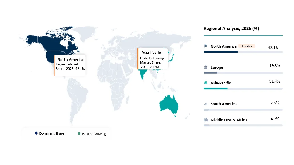
- The Asia-Pacific region held 42.1% of the global Chiplet Testing Market share in 2025 due to the presence of major semiconductor foundries, OSATs, advanced packaging facilities and chip manufacturing hubs in Taiwan, China, South Korea and Japan.
- The transition from monolithic semiconductor designs to modular chiplet architectures is increasing the adoption of multi-stage validation workflows, including Known Good Die (KGD), die-to-die interconnect, package-level and system-level testing, making advanced testing a critical part of semiconductor manufacturing.
- Package-Level Testing held around 23.8% of the global market share in 2025, making it the largest testing stage because of increasing advancements in packaging solutions and heterogenous chiplet integration.
- The Die-to-Die Interconnect Testing market is expected to register a CAGR of 16.9% between 2026 and 2035 due to the proliferation of UCIe chiplets, 2.5D/3D packaging and HBM-based semiconductor products.
- Increasing popularity of heterogeneous integration, hybrid bonding and advanced packaging processes is contributing to greater complexity of semiconductor validation requirements, creating consistent demand for precise chiplet testing solutions.
Chiplet Testing Industry Trends and Strategic Insights
- Shift in design approach from monolithic SoC-based designs towards chiplet-based architectures will change testing paradigms, making known good die (KGD) testing and die-to-die interconnect verification a critical step for chip manufacturers.
- With advanced packaging such as 2.5D ICs, 3D ICs, fan-out wafer-level packaging (FOWLP) and hybrid bonding are driving the adoption of high-precision testing and inspection platforms.
- Machine learning and artificial intelligence have been applied in ATEs and inspection equipment for optimizing tests, accelerating defect classification and improving yield rates.
- Collaboration between semiconductor manufacturers, foundries, OSATs and EDA tool makers is promoting standardized design-for-test (DFT) methodologies and chiplet ecosystem interoperability.
- Strategic investments in advanced semiconductor manufacturing, assembly and test capabilities in North America and Asia Pacific are increasing chiplet test capability and building supply chain resilience.
Chiplet Testing Market Scope
| Metrics | Details | |
| 2025 Market Size | US$ 1.27 Billion | |
| 2035 Projected Market Size | US$ 4.69 Billion | |
| CAGR (2026-2035) | 13.7% | |
| Largest Market | Asia-Pacific | |
| Fastest Growing Market | Asia-Pacific | |
| By Testing Stage | Wafer-Level Testing, Known Good Die (KGD) Testing, Die-to-Wafer Testing, Wafer-to-Wafer Testing, Die-to-Die Interconnect Testing, Package-Level Testing, Final Testing, System-Level Testing (SLT) and Burn-In & Reliability Testing | |
| By Test Type | Electrical Testing, Functional Testing, Parametric Testing, Structural Testing, Reliability Testing, Signal Integrity Testing and Thermal Testing | |
| By Packaging Technology | 2D Packaging, 2.5D IC Packaging, 3D IC Packaging, Fan-Out Wafer-Level Packaging (FOWLP), System-in-Package (SiP), Embedded Multi-die Interconnect Bridge (EMIB), Bridge-Based Packaging and Hybrid Bonding | |
| By Integration Type | Homogeneous Integration and Heterogeneous Integration | |
| By Chiplet Type | Compute Chiplets, Memory Chiplets, DRAM Chiplets, HBM Chiplets, NAND Chiplets, MRAM Chiplets, I/O Chiplets, Analog & Mixed-Signal Chiplets, RF Chiplets, Accelerator Chiplets, Security Chiplets, FPGA Chiplets and Others | |
| By Equipment | Automatic Test Equipment (ATE), Wafer Probers, Probe Cards, Test Handlers, Burn-In Systems and Inspection & Metrology Equipment | |
| By Service Model | In-House Testing and Outsourced Testing | |
| By End-User | Integrated Device Manufacturers (IDMs), Fabless Semiconductor Companies, Foundries, Outsourced Semiconductor Assembly & Test (OSAT) Providers and TIC Companies | |
| By Application | Artificial Intelligence (AI), High-Performance Computing (HPC), Data Centers & Cloud Computing, Consumer Electronics, Automotive, Telecommunications, Industrial, Aerospace & Defense, Healthcare and Others | |
| By Region | North America | U.S., Canada, Mexico |
| Europe | Germany, UK, France, Spain, Italy, Poland | |
| Asia-Pacific | China, India, Japan, Australia, South Korea, Indonesia, Malaysia, Singapore, Vietnam, Thailand, Philippines, Taiwan | |
| South America | Brazil, Argentina | |
| Middle East and Africa | UAE, Saudi Arabia, South Africa, Israel, Turkiye | |
| Report Insights Covered | Competitive Landscape Analysis, Company Profile Analysis, Market Size, Share, Growth | |
Why does this report matter in 2026?
The year 2026 marks a critical stage for the semiconductor industry because of the increasing use of chiplets in the development of processors in the field of artificial intelligence (AI), HPC systems, cloud computing, networking and automobile electronics. As the industry moves towards heterogeneous integration instead of monolithic integration in several high-performance applications, testing of KGDs, die-to-die connections and advanced packages becomes increasingly complex. In addition, with the growing use of UCIe ecosystem and advanced packaging, such as 2.5D ICs, 3D ICs and hybrid bonding, is driving demand for more sophisticated testing methodologies, high-precision Automatic Test Equipment (ATE) and AI-assisted inspection platforms.
This report offers valuable insights to stakeholders about the influence of technology advancements, competitive analysis, investment patterns and capacity building in various regions that would shape the Chiplet Testing Market in 2026. The report studies the influence of investments in advanced packaging, increases in OSAT capacity, expansion in semiconductor manufacturing and next-generation testing solutions on the market opportunity. This comprehensive report offers insights through its segmentation and analysis to enable equipment manufacturers, semiconductor manufacturers, foundries, investors and policymakers to capitalize on growth opportunities in the chiplet testing space.
Chiplet Testing Market White Space & Investment Opportunities
- The commercialization of standardized testing solutions for interoperable chiplet-based ecosystems becomes a great opportunity in the context of the growing popularity of UCIe and other open interconnect standards.
- The expansion of facilities for testing sophisticated chips in semiconductor production hotspots, including India, Southeast Asia and Europe, presents good opportunities for investment and diversification of global testing capacity.
- The development of platforms for automated testing using AI provides an opportunity for improving defect detection, testing coverage and minimizing testing costs of sophisticated multi-chip devices.
- An increase in the need for testing technologies capable of testing devices that support 2.5 D IC, 3 DvIC, hybrid bonding and HBM package results in new revenue streams for testing equipment makers and OSAT companies.
- Innovations in high-density probe cards, wafer probe technology and next-generation Automatic Test Equipment (ATE) enables vendors to address the growing testing complexity of AI, HPC and data center processors.
Chiplet Testing Future Market Transformation
The Chiplet Testing Market is expected to transform from conventional semiconductor validation into an intelligent, data-driven manufacturing function as chiplet-based architectures become mainstream. Future testing environments will integrate AI-powered analytics, adaptive test algorithms, digital twins and predictive quality monitoring to optimize test coverage, reduce cycle times and improve defect detection, process control and Known Good Die (KGD) identification. The emergence of standard chiplet interconnect ecosystem in terms of UCIe would support the development of testing processes that would promote collaboration among multiple vendors’ chiplets, while innovations in 2.5D/3D integration, hybrid bonding and high bandwidth memory (HBM) would necessitate next generation ATE systems to validate the more complex heterogeneous packages. Advanced packaging capacity and automation at semiconductor manufacturers and OSATs would make chiplet testing a critical tool for increasing manufacturing efficiency and enhancing supply chain resilience for next generation semiconductors.
Chiplet Testing Market Buyer Decision-Making Criteria
With the increasing complexity of chiplet architecture in semiconductors, the purchasing decision is now increasingly driven by the need for testing tools that guarantee high yield, reliability and scalability in advanced packaging technologies. Decision-makers evaluate testing platforms for their accuracy in identifying known good dies (KGDs), compatibility with heterogeneous integration and capability to validate high-speed die-to-die interconnects. Production efficiency, interoperability with the current manufacturing system, automation and reduction in the total cost of test are some of the factors that can influence the purchasing decision. Vendors with scalable Automatic Test Equipment, analytical solutions and excellent technical support are well placed to meet these needs.
Major Buyer Decision-Making Criteria
- Testing accuracy and known good die (KGD) yield
- Compatibility with 2.5D/3D ICs, hybrid bonding and advanced packaging
- High-speed die-to-die interconnect validation capability
- Test throughput and production scalability
- Integration with existing Automatic Test Equipment (ATE) and manufacturing workflows
- Support for heterogeneous integration and UCIe-based chiplet architectures
- Cost of Test (CoT) and overall return on investment (ROI)
- Measurement precision, reliability and repeatability
- Vendor technical expertise, global service and application support
- Future upgradeability and compatibility with next-generation chiplet technologies
Chiplet Testing Market Economic & Investment Analysis
The Chiplet Testing Market is experiencing robust economic momentum as semiconductor manufacturers increase capital expenditure on advanced packaging, heterogeneous integration and next-generation testing infrastructure. The growing complexity of chiplet-based devices has increased the economic importance of high-yield manufacturing, making investments in known good die (KGD) validation, advanced Automatic Test Equipment (ATE) and high-precision inspection systems essential for reducing the cost of test (CoT) and improving production efficiency. Incentives offered by governments to support the development of semiconductors and also to localize their supply chains in North America, Europe and the Asia Pacific region have boosted such investments.
In terms of investments, equipment makers, OSATs, foundries and semiconductor firms are investing in their capacity in the form of advanced testing, test automation using AI, wafer probing and reliability solutions. Strategic investments are now increasingly geared towards providing solutions for 2.5D/3D packaging, hybrid bonding and UCIe chiplets, which require increasing levels of testing. With an increasing demand for AI accelerators, HPC processors, automotive semiconductors and data center chips, those firms that can provide scalable and cost-effective testing solutions will be poised for better gains.
Chiplet Testing Investment Trends in the Market
- Semiconductor manufacturers are investing heavily in the development of the next generation of Automatic Test Equipment (ATE), wafer probers and metrology technology for chiplet-based semiconductor manufacturing.
- Advanced Packaging and OSAT firms and foundries are developing their advanced packaging and testing capabilities by investing in 2.5D/3D integration, hybrid bonding and mass-production facilities.
- Investments in AI-driven test automation, prediction analysis and digital testing solutions are rapidly growing to increase defect discovery efficiency, test coverage and decrease cost of test (CoT).
- Public and private investments in semiconductor programs help to develop local chiplet testing ecosystems by boosting domestic manufacturing and advanced packaging processes.
- Strategic partnerships and acquisitions between equipment providers, semiconductor companies, OSAT firms and EDA firms are boosting innovations in standardized chiplet testing technologies and interoperability.
Strategic Indicators For Chiplet Testing Market
High Regulation Impact
Compliance with standards such as AEC-Q100 standards for automotive semiconductors, functional safety standards, JEDEC standards for reliability testing and export control requirements have been contributing to the Chiplet Testing Market due to increasing quality standards for advanced chiplets. Growing adoption of heterogeneous integration, advanced packaging techniques and multi-vendor chiplet technology has led to the need for precise validation, automated test systems and traceability in order to ensure compliance. Consequently, regulatory compliance has evolved from a mandatory quality requirement into a strategic investment driver, accelerating the adoption of advanced chiplet testing technologies across AI, HPC, automotive and data center semiconductor applications.
High Investment Activity
The Chiplet Testing Market is characterized by increased levels of investments as semiconductor producers, testing equipment companies, foundries and OSATs speed up the process of developing future generation tests to ensure support for advanced architectures that chiplets have. Strategic investment of capital into testing processes is aimed at increasing high volume testing, expanding die-to-die connectivity tests, qualifying for reliability and increasing production throughput for advanced packaging. The focus of investment is moving towards scalable testing systems that can help realize the potential of heterogeneous integration and chiplet interoperability standards of the future. With chiplet technology gaining traction within artificial intelligence, HPC, automobile and networking industries, significant investment into testing capabilities has become the key source of competitive advantage.
Supply Chain Disruption
Market for Chiplet Testing is susceptible to medium to high disruption in the supply chain due to the dependency on special test equipment, high-end probe cards, high-grade substrates, sophisticated inspection machinery and advanced packaging supplies sourced from a few select vendors in the world. Additionally, the fact that the activities related to advanced packaging and OSAT take place in Asia and more specifically in Taiwan, South Korea and Southeast Asia adds to vulnerability. Any disruptions in this scenario could cause delays in the procurement of the equipment and slow down product qualification and lead to disruption in the provision of services associated with chiplet testing.
Pricing Volatility
There are moderate pricing risks associated with Chiplet Testing as more chiplet complexities and advances in packaging have resulted in continued pricing pressure on the procurement cost of testing equipment and supplies. The pricing levels of advanced Automatic Test Equipment (ATE), probe cards and inspection systems tend to be relatively volatile by varying between 5-15%, influenced by semiconductor demand, components shortages and technological shifts from one technology node to another in recent purchase cycles. On top of this, a narrow supplier base of advanced testing tools and advanced packaging materials poses further risk in terms of pricing. As a mitigation measure to such price pressures, semiconductor manufacturers and OSAT companies are entering into long-term purchase agreements and other cost management measures.
Procurement Pressure
There is increased procurement pressure in the Chiplet Testing Market with semiconductor companies, foundries and OSATs now requiring testing systems that will be able to accommodate different chiplet configurations, advanced packaging options and evolving inter-operability requirements. There are no longer only procurement of equipment concerns but also those regarding the lifecycle of procurement which includes software capabilities, ability to be upgraded, calibration needs and vendor knowledge and expertise. Buyers have adopted strict processes for qualifying their suppliers, procurement contracts and even multi-sourcing procurement processes so as to have continuity of technology and minimize risks to production of advanced semiconductor devices.
New Technology Adoption
There is an accelerated pace of implementation of the latest testing technologies within the market of the Chiplet Testing due to the increasing complexity of architectures based on chiplets and the need for heterogeneous integration by semiconductor companies. The advanced Automatic Test Equipment (ATE), artificial intelligence-based technology of defect detection, testing of interconnections at the high-speed die-to-die level, high-precision wafer probe testing and system-level testing are gradually becoming key components of the next generation of testing processes within the Chiplet Testing market. At the same time, the application of the interoperability standards according to UCIe, 2.5D/3D packaging, hybrid bonding and high bandwidth memory (HBM) stimulates the development of more advanced testing approaches.
Regional Expansion Opportunity
The Chiplet Testing Market offers strong regional expansion opportunities as semiconductor manufacturing and advanced packaging technology continue to diversify beyond traditional production hubs. Even though Taiwan, South Korea, China and Japan are still the main countries for chiplet manufacturing and testing, countries like India, Malaysia, Vietnam, Singapore, the US and Germany are building their semiconductor manufacturing ecosystem with new semiconductor manufacturing plants, advanced packaging solutions and OSAT expansion. The geographic diversification creates new opportunities for test equipment manufacturers, inspection solution companies and testing services to set up localized operations, reduce the time needed for customer support and build the local supply chain at the same time.
Government Policy Support
The Chiplet Testing Market is benefiting from strong government policy support as semiconductor testing and advanced packaging become strategic priorities within national semiconductor development programs. Regulatory actions by governments, semiconductor R&D activities, technology standardization efforts and skills development for workers are being encouraged to increase domestic capabilities in testing technologies. Governmental policies to promote semiconductor ecosystem resilience, technological innovation, technology commercialization and partnerships among the industry, academia and research organizations are contributing towards the development of a conducive environment for the testing of chiplets.
Pricing Intelligence
Pricing intelligence is becoming the norm in the Chiplet Testing Market as semiconductors manufacturers, foundries and OSATs compare various testing options for economic value in the long run as opposed to cost on first purchase. The performance of testing machines, test efficiency, improved yield, software licensing, maintenance service agreements and scalability are among the parameters being used to make sure the TCO is optimal. Premium chiplet testing solutions generally tend to fetch between 15-25% more money compared to traditional semiconductor testing systems. Nonetheless, their capability of improving manufacturing yields, cutting test times and testing numerous chiplet designs usually makes them a better option over the long haul.
| HS Code | Reporter | Trade Flow | 2025 Trade Value | Interpretation |
8486.40 (Machines and apparatus for manufacturing/testing semiconductor devices) | China | Imports | US$ 5.84 Billion | Reflects China's continued investments in semiconductor fabrication, advanced packaging and testing equipment, supporting demand for chiplet testing technologies. |
9030.82 (Electronic measuring and testing instruments) | United States | Imports | US$ 2.76 Billion | Indicates strong procurement of precision semiconductor test and measurement equipment for AI, HPC and advanced chip manufacturing. |
9031.80 (Measuring or checking instruments and machines) | Taiwan | Imports | US$ 3.41 Billion | Demonstrates sustained investment by Taiwan's foundries and OSAT providers in inspection, metrology and chiplet testing infrastructure. |
8542.31 (Electronic integrated circuits – Processors and controllers) | South Korea | Exports | US$ 42.85 Billion | Highlights South Korea's leadership in advanced semiconductor exports, reinforcing demand for high-reliability chiplet testing throughout the manufacturing process. |
AI Impact Analysis of Chiplet Testing Market
AI plays a significant role in changing the face of Chiplet Testing Market by improving testing efficiency, accelerating product qualification and enhancing manufacturing yield across increasingly complex semiconductor devices. Through analytical techniques supported by AI, defects are more quickly identified, tests are efficiently covered and predictive quality analysis becomes easier thanks to the ability to analyze large amounts of test data at wafer level, package level and systems level. All of this leads to decreased numbers of false failures, KGD quality improvement and a reduction in the Cost of Test (CoT).
In addition to improving manufacturing processes, the AI technology is also promoting the uptake of chiplet architectures through facilitating dependable validation of integration of different parts, fast interconnects between dies and advanced packaging technologies, such as 2.5D ICs, 3D ICs, hybrid bonding and chiplet ecosystems that utilize the UCIe standard. With continuing demands of AI processors to develop increasingly efficient semiconductors, there will be rising calls for intelligent testing methodologies, thus placing AI as an essential contributor in the future Chiplet Testing Market.
Disruption Analysis of Chiplet Testing Market
The Chiplet Testing Market is witnessing radical changes as the semiconductor industry moves from monolithic ICs to modular chiplet ICs. Chiplet based semiconductor testing differs greatly from traditional single IC tests due to the need for validation at different stages Known Good Die (KGD), die-to-die connection analysis, advanced package test and systems validation. Heterogeneous integration, 2.5D/3D IC packaging technology, hybrid bonding and UCIe supported chiplet ecosystem is adding complexities to the testing of multi-die semiconductors.
Disruption also continues to re-engineer the semiconductor industry value chain through changes to qualifications, interoperability needs and QA processes involving equipment makers, foundries, OSATs and silicon architects. Validation itself is being transformed from a discrete manufacturing phase into a continuous operation in the context of wafer production, advanced packaging, assembly and final systems qualification. Therefore, firms are moving fast towards creating chiplet validation ecosystems for improving qualification times, manufacturing yields and commercialization of cutting-edge AI, HPC, automotive and networking semiconductors.
Chiplet Testing Market BCG Matrix: Company Evaluation
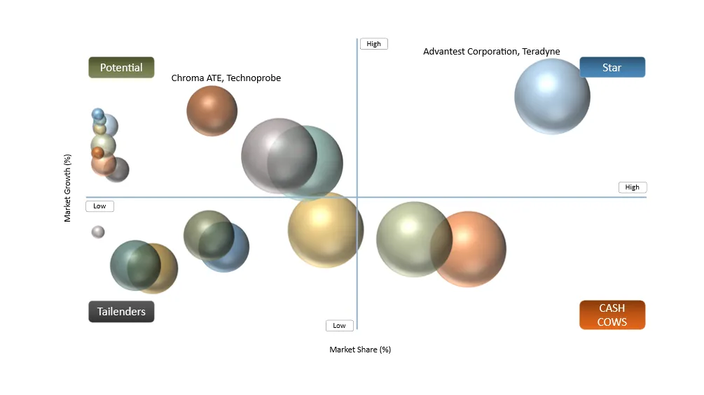
STAR
Advantest Corporation, Teradyne, FormFactor, ASE Technology Holding and Amkor Technology have been identified in the star quadrant because of their strong presence in the market and their capabilities in terms of providing various kinds of semiconductor testing services. With their strong focus on KGD validation, advance packaging, high volume semiconductor testing services, along with their ongoing efforts for developing new chiplet testing technologies, they are leaders in the rapidly growing chiplet testing market.
POTENTIAL
Potential quadrante includes Chroma ATE, Technoprobe, Cohu, Onto Innovation and Camtek due to their enhanced technologies as well as involvement in advanced solutions in relation to semiconductor testing, inspection, metrology and probes. With an ever-increasing need for heterogenous integration, 2.5D/3D packaging, hybrid bonding and chiplet designs enabled by UCIe interface, the aforementioned firms are ready for further market penetration by innovation and diversification into advanced chiplet testing solutions.
Chiplet Testing Market Dynamics
Driver Impact Analysis
| Driver | Market Growth Impact (%) | Demand Concentration | Impacted Use Case | Strategic Impact |
Rising Adoption of Chiplet- Based AI & HPC Processors | 28.40% | High in North America and Asia-Pacific | AI accelerators, HPC processors, data center chips | Drives investment in advanced wafer-level and known-good-die (KGD) testing solutions |
Expansion of Advanced Packaging Technologies (2.5D/3D, FOWLP, Hybrid Bonding) | 24.10% | Strong in Taiwan, South Korea, Japan and the U.S. | High-bandwidth memory (HBM), heterogeneous integration | Increases demand for interconnect validation, package-level testing and inspection technologies |
Growing Demand for Automotive & Edge Computing Semiconductors | 18.70% | Europe, China, Japan and North America | ADAS, autonomous driving, industrial edge AI | Accelerates adoption of high-reliability and burn-in testing for safety-critical devices |
Increasing Adoption of UCIe and Heterogeneous Integration Standards | 16.50% | Global semiconductor ecosystem | Multi-vendor chiplet integration, networking, telecom | Encourages development of standardized chiplet test methodologies and next-generation ATE platforms |
Driver: Rising Adoption of Chiplet-Based Architectures in AI and High-Performance Computing
The increasing adoption of chiplets within various technology applications, including AI, HPC, data centers, automotive electronics and advanced networking, is one of the main factors that fuel the Chiplet Testing Market. As many semiconductor vendors move from monolithic integrated circuits to modular chiplets that are expected to increase performance and power efficiency and improve scalability and yield rate of production, the task of validation of multiple dies has become quite complex. With the help of 2.5D ICs, 3D ICs, Hybrid Bonding, High-Bandwidth Memory (HBM) and UCIe-compatible interfaces, there is an essential need in KGD validation, validation of interconnections between dies and overall package/system level validation that is aimed at verifying functionality and interoperability and ensuring reliability of semiconductor devices.
Restraint Impact Analysis
| Restraint | Drag on Market Growth (%) | Primary Impact Area | Impacted Use Case | Strategic Impact |
High Cost of Advanced Chiplet Test Equipment | 21.80% | Capital investment | AI accelerators, HPC processors | Increases entry barriers and delays expansion of advanced test capacity |
Lack of Standardized Chiplet Test Methodologies | 18.90% | Test development & interoperability | Multi-vendor heterogeneous chiplet integration | Slows ecosystem adoption and increases test validation complexity |
Complex Testing for 2.5D/3D Packaging and Die-to-Die Interconnects | 17.40% | Advanced packaging verification | HBM-enabled processors, high-performance computing | Extends test cycles and raises manufacturing costs |
Limited Availability of Skilled Test Engineers | 14.60% | Workforce & technical expertise | Advanced semiconductor testing, OSAT operations | Constrains deployment of next-generation testing solutions and automation initiatives |
Restraint: High Complexity and Cost of Advanced Chiplet Testing
Advanced chiplet testing is highly complex and costly, posing as one of the main constraints on the Chiplet Testing market. While traditional semiconductor components undergo testing at just a few stages during production, a chiplet architecture necessitates validation during multiple phases, such as known good die (KGD) testing, die-to-die connectivity analysis, package-level testing, reliability evaluation and system-level testing. Rising heterogeneity and increased need for 2.5D/3D packaging, hybrid bonding technology and UCIe chiplet ecosystem demand advanced ATE equipment, probe cards, inspection systems and innovative validation procedures. It further adds to testing costs, increases time-to-market periods and demands higher levels of expertise required to implement advanced testing systems. All this poses major adoption obstacles for small-scale semiconductor manufacturers and new entrant OSATs in the chiplet domain.
Chiplet Testing Market Segmentation Analysis
The global Chiplet Testing market is segmented based on the Testing Stage, Test Type, Packaging Technology, Integration Type, Chiplet Type, Equipment, Service Model, End-User, Application and region.
By Testing Stage
Package-Level Testing Leads the Market with Comprehensive Validation of Advanced Chiplet Packages
The Package-Level Testing held a leading position in the Chiplet Testing Market, contributing 23.8% to the global market revenue of 2025. It was mainly attributed to the high popularity of such advanced packages as 2.5D/3D IC package, heterogeneous integration, hybrid bonding, fan-out wafer-level packaging (FOWLP) and system-in-package (SiP), which all required electrical and mechanical testing before moving to the next step in the process. Considering that the complexity of semiconductor packages such as chiplets used in the AI accelerator, HPC processor, automotive semiconductor and networking devices is continuously growing, package-level testing will remain the largest testing phase in the industry.
By Testing Stage
Die-to-Die Interconnect Testing Emerges as the Fastest-Growing Segment with Expanding Chiplet Adoption
Die to Die Interconnect Testing is expected to grow at a CAGR of 16.9% from 2026-2035 due to the availability of UCIe-based chiplets and the integration of High Bandwidth Memory technology in heterogeneous packaging. With an increase in demand for fast communication through chiplets and faster data exchange with high signal integrity, the demand for die to die interconnect testing is expected to witness accelerated growth. The increasing use of modular chiplet architectures by semiconductor companies makes Die to Die Interconnect Testing one of the fastest-growing phases of testing in the industry.
Chiplet Testing Market Geographical Penetration
Taiwan Chiplet Testing Market Outlook
Taiwan is expected to continue being one of the leading marketplaces for chiplets' testing, thanks to its dominance in semiconductor manufacturing foundry services, cutting-edge packaging and outsourced semiconductor assembly & testing (OSAT). The highly developed ecosystem of the architecture based on chiplets, heterogeneous integration, 2.5D/3D packaging, CoWoS, SoIC, hybrid bonding and chiplet eco-systems utilizing UCIe standards drives the requirements for sophisticated KGD validation, die to die interconnect tests, packaging tests and systems tests.
Rapid growth in advanced packaging volumes, manufacturing of AI accelerators and HPC processors, as well as collaboration between foundries, OSAT suppliers and semiconductor designers will enhance the leading position of Taiwan within the worldwide chiplet testing ecosystem. As the use of chiplets grows all over the world, Taiwan is expected to become a critical hub for testing of future generations of semiconductors within the forecast period.
U.S. Chiplet Testing Market Landscape
The US Chiplet Testing Market is one of the major players when it comes to semiconductor innovations owing to the ecosystem of semiconductors that includes a lot of semiconductor companies, providers of testing equipment, research organizations and advanced packaging technologies. A fast development and adoption of chiplet technology for AI, HPC, data centers, automotive and military applications creates an extensive need for advanced known good die (KGD) testing, die to die interconnection testing, package level testing and system level testing. Continued efforts in domestic semiconductor manufacturing, advanced packaging and testing developments along with the proliferation of heterogeneous integration, 2.5D/3D packaging, hybrid bonding and UCIe based chiplet ecosystem increase the potential for high accuracy chiplet testing solutions in the country during the forecast period.
South Korea Chiplet Testing Market Outlook
The Chiplet Testing Market in South Korea is expected to continue being an important player owing to its world dominance in advanced memory semiconductors, AI processors and next-generation semiconductor fabrication.
Adoption of chiplet architecture is increasing rapidly within AI, HPC, data centers, automotive electronics and advanced network systems and this calls for increasingly complex and sophisticated processes of KGD validation, die-to-die connectivity validation, package level and system level testing. More usage of High Bandwidth Memory (HBM), heterogeneous integration, 2.5D / 3D packaging and hybrid bonding leads to even greater demands on testing process precision. As South Korea further develops semiconductor manufacturing infrastructure, it is anticipated to be a large market for next-generation chiplet testing services during the forecast period.
China Chiplet Testing Market Trends
The Chiplet Testing Market in China is rapidly growing owing to the rising adoption of chiplet technologies by local companies to improve computing efficiency and make their supply chains more robust. There is an increase in investments made by companies into new packaging solutions, greater OSAT capabilities, heterogeneous integration, 2.5D/3D packaging, hybrid bonding and Chiplet UCIe Architecture. One of the key trends in China's Chiplet Testing market is greater localization of semiconductors testing infrastructure with manufacturers developing better KGD testing methods, die-to-die interconnection testing and system level testing capabilities to support the needs of high performance computing systems, AI accelerator devices, automotive electronics and data centers. Due to continued development of local innovations in the semiconductor industry, China will be one of the fastest growing markets for advanced chiplet testing technologies in the forecasted period.
Japan Chiplet Testing Market Outlook
Japan is anticipated to stay a strategically vital market for the Chiplet Testing Market based on its proficiency in manufacturing equipment, inspection, probing technologies, metrology and material technologies for semiconductor packaging. The knowledge base for wafer-level inspection, reliability qualification and advanced semiconductor validation that Japan possesses is driving the adoption of chiplet technology within artificial intelligence, automotive, industrial and high-performance computing applications.
The increased usage of heterogeneity, 2.5D/3D packaging, hybrid bonding and UCIe chiplets is driving an increased need for chiplet testing technologies. As Japan develops its semiconductor manufacturing capabilities technologically and industrially, it is anticipated to stay an important market for chiplet testing in the upcoming forecast period.
Chiplet Testing Market Competitive Landscape
- The industry represents a moderately concentrated market with players competing in terms of technical expertise and accuracy, offering solutions for testing equipment for OSAT and other semiconductors.
- With the rise of complex chiplet structures, competition is increasingly associated with solutions and technologies related to known good die (KGD) testing, testing of die-to-die interconnects, packaging validation and system-level heterogeneities validation.
- Innovation in product is the main factor that sets companies apart from the competition, as they are implementing test analytics using AI technology, high-performance interfaces, precise metrology and automatic defect detection in order to increase yield, decrease test duration and decrease the cost of testing (CoT).
- Market positioning through partnerships and increased capacity has been another key strategy adopted by companies as they are forming alliances with foundries, OSATs and semiconductor producers and building more testing capacity to meet rising demand for chiplet solutions.
- The Asia Pacific is the center of attention when it comes to the competitive expansion of companies because of greater spending on application engineering, technical support and manufacturing capabilities.
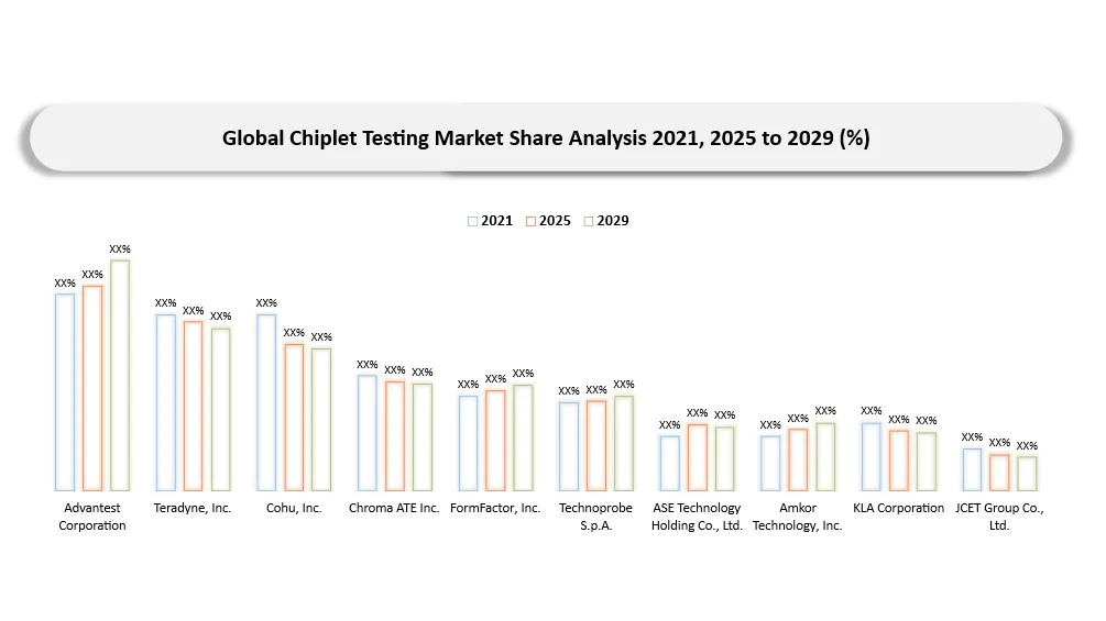
Chiplet Testing Market Key Companies
- Advantest Corporation (Japan)
- Teradyne, Inc. (United States)
- Cohu, Inc. (United States)
- Chroma ATE Inc. (Taiwan)
- FormFactor, Inc. (United States)
- Technoprobe S.p.A. (Italy)
- Micronics Japan Co., Ltd. (Japan)
- SPEA S.p.A. (Italy)
- MPI Corporation (Taiwan)
- Aehr Test Systems (United States)
- Onto Innovation Inc. (United States)
- Camtek Ltd. (Israel)
- KLA Corporation (United States)
- Tokyo Electron Limited (Japan)
- ASMPT Limited (Singapore)
- ASE Technology Holding Co., Ltd. (Taiwan)
- Amkor Technology, Inc. (United States)
- JCET Group Co., Ltd. (China)
- Powertech Technology Inc. (Taiwan)
- ChipMOS Technologies Inc. (Taiwan)
Chiplet Testing Market Major Pain Points
- Increasing Multi-Die Validation Complexity: It becomes necessary to validate Known Good Die (KGD), die-to-die connection, advanced packaging and chiplets assembly through different levels of validation, making it complex from an engineering standpoint, as well as from the test time point of view.
- High Cost of Advanced Testing Infrastructure: The testing of leading-edge chiplets necessitates expenditures for automatic test equipment, high density probe cards, advanced test tools and reliability testing tools, thereby increasing cost both in terms of capital and operations.
- Lack of Standardization in the Presence of Multiple Chiplet Platforms: The presence of multiple chiplet platforms, along with advanced packaging and interoperability standards, poses challenges in formulating standardized qualification and validation procedures.
- Difficult Fault Isolation in Multi-Chiplet Packages: Locating any fault in chiplets, fast communication interfaces and complex packages is more difficult than that in traditional single-piece semiconductors, making the process difficult for improving yield and conducting root cause analysis.
- Longer Qualification and Reliability Cycles: The lengthy testing process needed for validating advanced chiplet packages leads to a delay in qualification and subsequent high volume manufacturing.
Chiplet Testing Market Recent Developments
- February 2026: FormFactor Inc. developed vertical MEMS probes with sub-60 micron pitch for use in high-density chiplet packaging connections and wafer-level tests for future AI and HPC processor chips and advanced semiconductors.
- May 2026: Onto Innovation Inc. introduced the Dragonfly G5 platform with 3D inspection and measurement features of advanced interconnections and micro-bumps of less than 6 microns tall in chiplets.
- February 2026: Amkor Technology, Inc. declared capital investment of US$ 2.5 billion to improve High-Density Fan-Out (HDFO) and 2.5D chiplet testing and packaging plants in Arizona, enhancing its sophisticated semiconductor production capabilities.
- July 2026: ASE Technology Holding Co., Ltd. unveiled its Integrated Design Ecosystem (IDE), helping to improve chiplet packaging and testing processes and cut down the time needed for AI data center and high-performance computing uses.
- May 2026: Camtek Ltd. added hybrid bonding surface inspection and metrology solutions, as well as fine pitch microbump alignment for advanced chiplets and HBM (High-Bandwidth Memory) packages.
Analyst View / Opinion on Chiplet Testing Market
- The success of chiplet-based semiconductors from a business perspective in the longer term will depend not only on design but equally on testing innovation since advanced testing capabilities will play an essential role in ensuring competitive advantages for vendors across the semiconductor chain.
- Testing requirements will shift to more advanced testing solutions that can test Known Good Die (KGD), die-to-die connectivity, advanced packaging technologies and multi-chiplet modules through a unified qualification process.
- As the UCIe and heterogeneous chiplet ecosystems evolve, vendors which provide scalable and interoperable and standards-based test solutions will emerge as the preferred choice for testing multi-vendor chiplet integration.
- In future competitions, vendors who can reduce the Cost of Test (CoT) without compromising on quality will have the edge with intelligent test optimization, high throughput validation and defect location being critical success factors.
- Scalable testing capability for mass volume testing for AI accelerators, HPC CPUs, automotive semiconductors and networking semiconductors will set the vendors apart from others and drive future market leadership.
Chiplet Testing Market Target Audience
| INDUSTRY | WHO SHOULD BUY THIS REPORT? | REASON TO BUY THIS REPORT |
| Semiconductor Manufacturing | Semiconductor manufacturers, IDMs | Evaluate chiplet testing trends, investment opportunities and technology roadmaps |
| Test Equipment Manufacturing | ATE, probe card and inspection equipment manufacturers | Identify demand outlook, competitive landscape and emerging testing requirements |
| Outsourced Semiconductor Assembly & Test (OSAT) | OSAT service providers | Optimize testing capabilities and plan advanced packaging investments |
| Semiconductor Foundries | Foundry executives and process engineers | Understand testing requirements for heterogeneous integration and advanced packaging |
| Fabless Semiconductor Companies | Chip designers and product development teams | Benchmark testing strategies for chiplet-based product development |
| Automotive Electronics | Automotive semiconductor suppliers and Tier-1 manufacturers | Assess reliability testing needs for ADAS, EVs and autonomous vehicle applications |
| Data Center & AI Computing | AI accelerator developers, HPC vendors, cloud infrastructure providers | Track testing technologies supporting high-performance chiplet architectures |
| EDA & Design Software | EDA software vendors and DFT solution providers | Develop advanced design-for-test and chiplet verification solutions |
| Investment & Private Equity | Venture capital firms, private equity investors, institutional investors | Evaluate market growth potential, investment opportunities and competitive positioning |
| Government & Research Organizations | Government agencies, research institutes, industry associations | Support semiconductor policies, R&D initiatives and domestic chiplet ecosystem development |
Why Choose DATAM?
- Data-Driven insights: Dive into detailed analyses with granular insights such as pricing, market shares and value chain evaluations, enriched by interviews with industry leaders and disruptors.
- Post-Purchase Support and Expert Analyst Consultations: As a valued client, gain direct access to our expert analysts for personalized advice and strategic guidance, tailored to your specific needs and challenges.
- White Papers and Case Studies: Benefit quarterly from our in-depth studies related to your purchased titles, tailored to refine your operational and marketing strategies for maximum impact.
- Annual Updates on Purchased Reports: As an existing customer, enjoy the privilege of annual updates to your reports, ensuring you stay abreast of the latest market insights and technological advancements. Terms and conditions apply.
- Specialized Focus on Emerging Markets: DataM differentiates itself by delivering in-depth, specialized insights specifically for emerging markets, rather than offering generalized geographic overviews. The approach equips our clients with a nuanced understanding and actionable intelligence that are essential for navigating and succeeding in high-growth regions.
- Value of DataM Reports: Our reports offer specialized insights tailored to the latest trends and specific business inquiries. The personalized approach provides a deeper, strategic perspective, ensuring you receive the precise information necessary to make informed decisions. The insights complement and go beyond what is typically available in generic databases.
What DATAM Uniquely Provides
- Analysis of the entire testing value chain of chiplets, consisting of wafer testing, KGD testing, interconnection between dies, package-level testing, system-level testing and reliability testing throughout the entire semiconductor manufacturing process.
- Analysis of next-generation chiplets technologies such as heterogeneity, UCIe, 2.5D/3D packaging, hybrid bonding, CoWoS, SoIC and advanced substrate technologies and how they influence testing approach.
- Technology & Market Intelligence Report featuring strategic indicators, AI impact assessment, disruption potential, investment trends, price intelligence, procurement dynamics and supply chain analysis all in one place.
- Competitive analysis from a country perspective with regard to leading semiconductor clusters, stressing the importance of regional manufacturing, advanced packaging ecosystems, OSAT developments and technology trends that will affect the global chiplet testing arena.
- Decision-oriented analysis for semiconductor industry participants, offering practical advice with respect to technology adoption and testing infrastructure, ecosystem development and growth prospects.