Heterogeneous Integration Market Size and Overview
The global Heterogeneous Integration market is estimated at US$ 1.66 billion in 2025 and is expected to reach US$ 35.09 billion by 2035, expanding at a CAGR of 35.70% during 2026-2035. The market is moving from a specialist packaging layer into a core system architecture for AI accelerators, high-performance computing, networking, automotive electronics and photonic systems. The value pool is expanding across design IP, interposers, advanced substrates, hybrid bonding, high-bandwidth memory integration, equipment, materials, inspection and test.
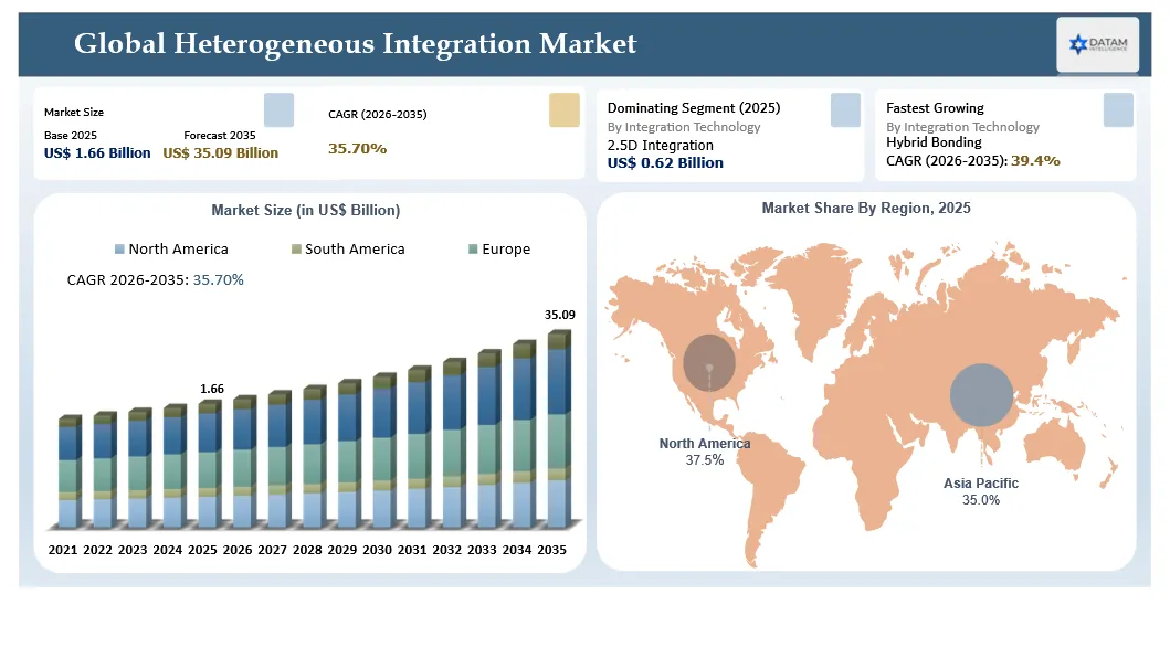
The market is being reshaped by a capacity race. More than US$600 billion of announced investment is flowing into twelve new U.S. semiconductor fabrication projects, while TSMC has raised its total planned U.S. commitment to US$265 billion. The U.S. buildout increasingly includes advanced packaging and supporting infrastructure because domestic wafer fabrication without local packaging leaves a critical part of the AI supply chain concentrated in Asia. TSMC also increased its 2026 capital spending guidance to US$60-64 billion as AI demand increased utilization of leading-edge logic and advanced packaging.
TSMC continues to position CoWoS, SoIC, InFO and photonic integration as central platforms. In June 2026, the company stated that wafer-level CoWoS still has room to scale to a package containing up to 58 large reticle-sized dies. Panel-level packaging offers a larger physical format, but its tool ecosystem and interconnect density remain less mature. TSMC expects a CoPoS pilot line during 2026, while broader commercial production is more likely around 2029-2030. This keeps wafer-level packaging central to near-term AI investment while opening a longer-term equipment and materials opportunity around panels.
From 2026 to 2035, commercial success will depend on package-level co-design, high-yield bonding, thermal management, substrate access, HBM supply, test coverage and open die-to-die connectivity. UCIe 3.0 expands the industry push toward interoperable chiplets, though qualification, security, reliability and multi-vendor business rules remain unresolved. Buyers will increasingly evaluate suppliers on system-level performance, capacity certainty and time-to-volume rather than individual process specifications.
| Metric | Details |
| 2025 Market Size | US$ 1.66 Billion |
| 2035 Projected Market Size | US$ 35.09 Billion |
| CAGR (2026-2035) | 35.70% |
| Largest Market | North America |
| Fastest Growing Market | Asia-Pacific |
| Largest Technology Segment | 2.5D integration and silicon interposer platforms |
| Fastest Growing Technology Segment | Hybrid bonding and 3D die stacking |
| Largest Application | AI accelerators and high-performance computing |
| Report Insights | Capacity, chiplet economics, HBM, interconnects, thermal design, equipment, materials, regional investment and competitive strategy |
Heterogeneous Integration Market Key Takeaways
- The market is estimated at US$ 1.66 billion in 2025 and projected to reach US$ 35.09 billion by 2035, supported by AI accelerator packages, chiplet reuse, HBM integration and advanced data-center networking.
- North America leads demand through hyperscaler spending, fabless semiconductor design, AI system companies and government-backed semiconductor localization.
- Asia-Pacific is the fastest growing region and the main manufacturing base, supported by Taiwan foundries and OSATs, South Korean memory suppliers, Japanese materials and equipment, and expanding capacity in China, Malaysia and Singapore.
- 2.5D integration remains the largest commercial platform because current AI processors depend on silicon interposers, advanced substrates and HBM stacks.
- Hybrid bonding and 3D stacking are the fastest growing technologies as bump pitch shrinks and designers seek higher bandwidth with lower interconnect energy.
- TSMC stated that CoWoS can scale to packages containing up to 58 large reticle-sized dies, indicating that wafer-level integration still has a substantial near-term roadmap.
- Panel-level packaging is emerging as a complementary route. Tooling, interconnect density, warpage control and process maturity remain barriers to replacing wafer-level systems for the largest AI packages.
- U.S. semiconductor manufacturing projects exceed US$600 billion across twelve new fabs, creating adjacent demand for domestic advanced packaging, substrates, equipment and skilled engineering.
- TSMC has raised its planned U.S. investment to US$265 billion and guided 2026 capital spending to US$60-64 billion, demonstrating the scale of AI-driven capacity requirements.
- Failure analysis is becoming a strategic bottleneck. A 2026 industry survey found that heterogeneous, chiplet and 3D products represented 69% of respondents, while 54% identified hybrid bonding as the hardest emerging architecture to analyze.
- UCIe 3.0 is accelerating the development of an open chiplet ecosystem, creating opportunities in controller IP, verification, security, interoperability testing and reusable die libraries.
- Long-term value will shift toward suppliers that combine packaging process capability with design enablement, thermal modeling, test, reliability and customer-specific system optimization.
Why does this report matter in 2026?
In 2026, heterogeneous integration is becoming the deciding constraint for AI processor delivery. Leading-edge wafers are only one part of the supply chain. AI accelerators also require HBM, interposers, advanced substrates, bonding equipment, thermal solutions and complex final test. Capacity shortages in any one layer can delay complete systems. The report helps buyers understand where capacity is being added, which technologies are ready for volume, where supplier concentration remains high and which alternative platforms can reduce exposure.
The report also matters because architecture choices are becoming investment decisions. CoWoS, EMIB, Foveros, I-Cube, X-Cube, fan-out, hybrid bonding and panel-level packaging have different cost, yield, density, thermal and ecosystem implications. Semiconductor companies need a commercial view of these trade-offs before committing product roadmaps. Equipment and materials suppliers need to identify where new process steps create recurring spending. Governments need to evaluate whether domestic packaging capacity is aligned with local wafer production and defense requirements.
Heterogeneous Integration Market White Space and Investment Opportunities
- Regional advanced-packaging capacity in the U.S., Europe, India and the Middle East, including interposer, substrate, assembly, inspection and test capability.
- Hybrid bonding tools, surface preparation, metrology and contamination control for fine-pitch 3D integration.
- High-performance substrates, glass cores, low-loss dielectrics, underfills, thermal interface materials and warpage-control materials.
- Chiplet IP libraries and UCIe-compatible interface controllers for compute, memory, I/O, security, power and analog functions.
- AI-assisted package co-design covering power delivery, thermal behavior, mechanical stress, signal integrity and yield optimization.
- Non-destructive inspection and failure analysis for buried interconnects, micro-bumps, TSVs and hybrid-bonded interfaces.
- Co-packaged optics and photonic-electronic integration for scale-up and scale-out AI networks.
- Panel-level process equipment, temporary bonding, redistribution, lithography and handling systems for the post-2029 capacity cycle.
Heterogeneous Integration Future Market Transformation
The market will evolve from package assembly toward system technology co-optimization. Logic, memory, I/O, photonics and power delivery will be selected as modular building blocks, with packaging architecture decided alongside the chip design. This creates a larger role for EDA vendors, interface IP providers, thermal engineers and test specialists. Foundries and OSATs will compete through integrated design enablement, qualified chiplet ecosystems and guaranteed capacity.
Wafer-level packaging will remain central through the current AI investment cycle. Panel-level packaging will gain relevance where larger form factors and throughput can offset lower interconnect density. The most likely market outcome is coexistence. CoWoS and related wafer-level platforms will serve the most demanding processors, while panels may first scale in less dense packages, large substrates, networking and selected accelerator architectures.
Heterogeneous Integration Market Buyer Decision-Making Criteria
Buyers evaluate heterogeneous integration platforms through bandwidth density, interconnect energy, thermal resistance, package size, known-good-die strategy, yield, testability, substrate availability, qualification time and capacity assurance. AI companies prioritize HBM integration, power delivery and thermal performance. Automotive buyers place greater weight on reliability, lifecycle supply and qualification. Photonics buyers assess optical coupling, thermal stability and co-packaged assembly. Government and defense buyers add trusted supply and regional manufacturing requirements.
Procurement teams increasingly request multi-year capacity commitments, second-source strategies, detailed yield learning plans and transparent material sourcing. A technically attractive package can still lose a design if it depends on one substrate supplier or lacks scalable test. Winning suppliers support design migration, package simulation, prototype builds and manufacturing ramp through one commercial relationship.
Heterogeneous Integration Market Economic and Investment Analysis
Investment is spreading across fabs, packaging plants, OSAT capacity, substrates, equipment and materials. The U.S. semiconductor manufacturing buildout has exceeded US$600 billion across twelve new fab projects. TSMC has increased its total U.S. commitment to US$265 billion, while its 2026 capital expenditure guidance rose to US$60-64 billion. These investments support a broader localization opportunity for advanced packaging because AI products require closely coordinated wafer and package supply.
The attractive targets are businesses with qualified process IP, scarce equipment positions, proprietary materials, established hyperscaler relationships or deep test capability. Risks include rapid technology migration, customer concentration, long qualification periods, cyclic capital spending and underutilized capacity. Investors should distinguish between commoditized assembly and process steps that control yield, density, thermal performance or system qualification.
Strategic Indicators for Heterogeneous Integration Market
High Regulation Impact
Export controls, CHIPS incentives, trusted supply requirements and national-security policies influence where advanced packaging can be built and which customers can access leading technologies.
High Investment Activity
Foundries, OSATs and equipment suppliers are increasing spending on CoWoS, hybrid bonding, fan-out, advanced substrates, inspection and test.
Supply Chain Disruption
HBM, substrates, interposers, bonding tools and specialist materials can become package-level bottlenecks even when wafer capacity is available.
Pricing Volatility
Package pricing reflects substrate supply, HBM availability, yield learning, mask and NRE costs, equipment utilization and customer-specific engineering.
Procurement Pressure
AI customers require reserved capacity, faster ramps, known-good-die control and clear package roadmaps across multiple accelerator generations.
New Technology Adoption
Hybrid bonding, UCIe, glass substrates, optical I/O, backside power and AI-assisted inspection are entering commercial roadmaps.
Regional Expansion Opportunity
North America leads demand, while Asia-Pacific remains the core manufacturing region. Europe, India and the Middle East are building strategic capability.
Government Policy Support
CHIPS programs, tax credits and national semiconductor strategies support local fabs, packaging, R&D, workforce and supply-chain resilience.
Heterogeneous Integration Market Dynamics
Driver Impact Analysis
| Driver | Market Growth Impact | Demand Concentration | Impacted Use Case | Strategic Impact |
| AI accelerator and HPC demand | 29% | U.S., Taiwan, South Korea | 2.5D logic plus HBM | Makes packaging capacity a direct constraint on accelerator shipments |
| Chiplet economics and design reuse | 23% | Global fabless and system companies | Modular compute, I/O and memory | Reduces dependence on one monolithic die and enables node optimization |
| HBM and memory bandwidth growth | 19% | AI and data-center markets | CoWoS, interposers, 3D memory | Raises demand for interposers, substrates, bonding and thermal solutions |
| Regional capacity localization | 16% | U.S., Europe, India, Japan | Trusted and resilient packaging | Creates new plants, equipment demand and supplier localization |
| Open interconnect standards | 13% | Global chiplet ecosystem | UCIe-based multi-vendor systems | Expands interface IP, validation and reusable chiplet markets |
Driver: AI and HPC Pull Advanced Packaging Into the Critical Path
AI processors require combinations of leading-edge logic, multiple HBM stacks, high-density interconnects and increasingly complex power delivery. The packaging step now determines how much compute and memory can be assembled into one system. TSMC’s statement that CoWoS can scale to as many as 58 large reticle-sized dies illustrates how far system complexity can move beyond the boundaries of a monolithic reticle. The commercial result is sustained spending on interposers, advanced substrates, lithography, bonding, inspection, thermal materials and package-level test.
Restraint Impact Analysis
| Restraint | Drag on Growth | Primary Impact Area | Impacted Use Case | Strategic Impact |
| Yield and known-good-die risk | 22% | Multi-die assembly | Large AI packages | One defective die can destroy substantial package value |
| Thermal and power density | 19% | AI and 3D stacks | HPC and networking | Limits achievable integration density and system reliability |
| Substrate and equipment concentration | 17% | Supply assurance | CoWoS, fan-out and 3D | Extends lead times and increases customer reservation requirements |
| Test and failure analysis complexity | 15% | Qualification and ramp | Hybrid bonding and buried interfaces | Slows yield learning and raises engineering cost |
| Standards and business-model gaps | 12% | Multi-vendor chiplets | Open UCIe ecosystems | Limits plug-and-play procurement despite technical progress |
Restraint: Yield, thermal, and test complexity increase with every added die.
Heterogeneous systems multiply interfaces, materials and process interactions. Warpage, micro-bump defects, voids, TSV failures, bonding contamination and thermal gradients may appear only after assembly. A 2026 industry survey found that 69% of respondents worked with heterogeneous, chiplet or 3D products, 54% identified hybrid bonding as the hardest emerging architecture to analyze and 83% supported formalized data standards. This creates a strong opportunity for inspection and analytics, but it also raises qualification cost and can slow commercial ramps.
Heterogeneous Integration Market Segment Analysis
By Integration Technology: 2.5D Integration Retains the Largest Commercial Base
2.5D platforms remain the largest segment because they combine logic and HBM through silicon interposers or advanced bridges without requiring every die to be vertically stacked. CoWoS, EMIB and similar platforms have mature customer roadmaps and established manufacturing ecosystems. The growth opportunity remains large because AI packages are increasing in die count, interposer area and memory content. Hybrid bonding and direct 3D stacking will grow faster where interconnect pitch and energy are critical.
By Packaging Platform: Wafer-Level Systems Lead the Near-Term AI Cycle
Wafer-level platforms offer the interconnect density and mature tooling required for the largest AI processors. TSMC has argued that panel-level packaging will complement rather than immediately replace CoWoS. Panels can reach larger physical formats, but tools, warpage control and density need further development. The first CoPoS pilot line is expected during 2026, with broader production closer to 2029-2030.
By Component: Logic and HBM Create the Largest Value Pool
Compute chiplets and HBM stacks account for the largest package value because AI systems need large memory bandwidth and dense logic-memory communication. I/O chiplets, security dies, power management and optical engines create the next growth layer by enabling modular architecture and specialized process-node selection.
By Interconnect: Hybrid Bonding Is the Fastest Growing Route
Micro-bumps remain widely used, but hybrid bonding is gaining importance as pitch shrinks and interconnect energy becomes a system bottleneck. The opportunity extends beyond bonding tools to wafer preparation, planarization, cleaning, metrology, alignment, inspection and failure analysis.
By Application: AI Accelerators and HPC Dominate Demand
AI and HPC are the largest applications because accelerator packages combine leading-edge compute, multiple HBM stacks and high-density interposers. Data-center networking, co-packaged optics and custom hyperscaler silicon create adjacent demand. Automotive and industrial systems adopt heterogeneous integration more slowly but provide longer lifecycle revenue.
By End User: Foundries and OSATs Build Competing Integration Ecosystems
Foundries compete through tightly integrated wafer and package roadmaps, while OSATs provide broader customer access, lower-volume flexibility and multi-foundry assembly. Hyperscalers and fabless companies increasingly influence package technology roadmaps and reserve capacity directly.
By Business Model: Co-Design and Turnkey Services Gain Share
The market is shifting from assembly-only contracts toward co-design, simulation, substrate development, test planning and lifecycle capacity support. Turnkey suppliers can capture more value and reduce customer coordination risk. Chiplet IP licensing and open ecosystem models will grow as UCIe adoption expands.
Heterogeneous Integration Market Geographical Penetration
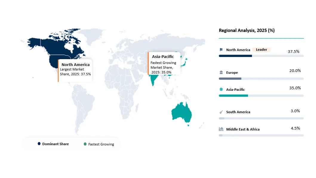
North America Heterogeneous Integration Market Outlook
North America leads market value through AI accelerator design, hyperscaler spending, advanced EDA, equipment leadership and government-backed manufacturing. The U.S. semiconductor construction pipeline exceeds US$600 billion across twelve new fab projects. TSMC’s planned U.S. investment has reached US$265 billion. The next gap is packaging depth. Domestic demand will support advanced assembly, substrates, testing, photonics and trusted defense supply.
Asia-Pacific Heterogeneous Integration Market Landscape
Asia-Pacific is the manufacturing center and fastest growing region. Taiwan leads foundry packaging through TSMC and OSAT capacity. South Korea contributes HBM, memory and advanced packaging. Japan provides substrates, chemicals, equipment and materials. China is investing in domestic packaging and chiplet capability. Malaysia and Singapore support OSAT, test and regional supply diversification.
Europe Heterogeneous Integration Market Outlook
Europe combines automotive semiconductor demand, equipment leadership, research institutes and advanced manufacturing programs. Germany, France, the Netherlands and Belgium are important for automotive, lithography, photonics, R&D and packaging equipment. European opportunities concentrate on chiplets for automotive and industrial systems, photonics, power electronics and sovereign semiconductor programs.
South America Heterogeneous Integration Market Outlook
South America remains an emerging demand market with limited advanced-packaging capacity. Brazil offers opportunities in design services, research, automotive electronics and selected back-end assembly. Market entry depends on partnerships, workforce development and links to North American or Asian manufacturing ecosystems.
Middle East and Africa Heterogeneous Integration Market Outlook
The Middle East is exploring semiconductor investment through sovereign funds, AI infrastructure and technology localization. Israel has strong semiconductor design and packaging R&D. UAE and Saudi Arabia can support future design centers, advanced test and strategic investment. Near-term opportunity is strongest in capital, partnerships and specialized engineering rather than high-volume manufacturing.
| Region/Country | Primary Opportunity | Buyer-Intent Insight |
| U.S. | AI packaging, chiplet IP, equipment, domestic OSAT and trusted supply | Buyers prioritize capacity assurance, security and system-level co-design |
| Taiwan | CoWoS, SoIC, OSAT, substrates and volume manufacturing | Scale and ecosystem depth remain unmatched, but capacity concentration is a concern |
| South Korea | HBM, memory integration and advanced substrates | Growth follows AI memory content and vertical integration |
| Japan | Materials, equipment, substrates and hybrid bonding | Suppliers benefit from high qualification barriers and customer trust |
| China | Domestic advanced packaging and chiplet platforms | Localization supports demand, while export controls constrain tool access |
| Germany/Netherlands | Automotive chiplets, photonics, lithography and equipment | Opportunity is specification-led and linked to European sovereignty |
| India | OSAT, assembly, design services and government-supported capacity | Best suited for new regional capacity and workforce-led expansion |
| Malaysia/Singapore | OSAT, test, logistics and regional diversification | Buyers seek scalable back-end capacity outside Taiwan and China |
Heterogeneous Integration Market Competitive Landscape
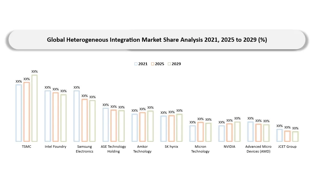
- TSMC competes through CoWoS, InFO, SoIC and integrated foundry-packaging roadmaps aligned with the largest AI customers.
- Intel Foundry uses EMIB and Foveros to differentiate through embedded bridges and vertical stacking, while expanding external foundry access.
- Samsung combines leading-edge logic, memory and advanced packaging through I-Cube and X-Cube, creating a vertically integrated alternative.
- ASE, Amkor and JCET compete through broad customer access, OSAT scale, advanced system-in-package and regional manufacturing footprints.
- Equipment suppliers are moving closer to package architecture because bonding, deposition, etch, lithography, inspection and metrology determine yield.
- EDA vendors are expanding package co-design, multi-die verification, thermal analysis and chiplet interface workflows.
- Substrate and material suppliers gain pricing power where qualification and capacity are concentrated.
- UCIe and open chiplet standards create room for new IP vendors, interoperability labs and reusable chiplet marketplaces.
Key Companies of Heterogeneous Integration Market
- TSMC (Taiwan)
- Intel Foundry (United States)
- Samsung Electronics (South Korea)
- ASE Technology Holding (Taiwan)
- Amkor Technology (United States)
- JCET Group (China)
- SK hynix (South Korea)
- Micron Technology (United States)
- Broadcom (United States)
- NVIDIA (United States)
- AMD (United States)
- Applied Materials (United States)
- Lam Research (United States)
- KLA (United States)
- BESI (Netherlands)
- Cadence Design Systems (United States)
- Synopsys (United States)
- Siemens EDA (United States)
- Ibiden (Japan)
- Unimicron (Taiwan)
Heterogeneous Integration Market Major Pain Points
- Advanced-packaging capacity remains concentrated among a small number of foundries and OSATs.
- Large AI packages combine expensive logic and HBM, making yield loss financially severe.
- Thermal density and power delivery limit integration before interconnect density reaches its theoretical maximum.
- Substrate, interposer and HBM shortages can delay complete systems despite available logic wafers.
- Failure analysis is difficult because critical interfaces are buried inside 2.5D and 3D structures.
- Multi-vendor chiplet standards are progressing faster than commercial liability, warranty and qualification frameworks.
- Package design requires cross-domain engineering across silicon, substrate, power, thermals, mechanics and test.
- Regional localization is expensive because advanced packaging needs specialized equipment, materials, workforce and customer qualification.
Heterogeneous Integration Market Recent Developments
- July 2026: TSMC announced an additional US$100 billion U.S. expansion, increasing its total planned U.S. investment to US$265 billion. The plan includes four additional advanced fabs and supporting capacity.
- July 2026: TSMC raised 2026 capital expenditure guidance to US$60-64 billion as AI demand increased leading-edge logic and packaging requirements.
- July 2026: U.S. semiconductor manufacturing investment exceeded US$600 billion across twelve new fab projects, supporting equipment, construction and advanced-packaging demand.
- June 2026: TSMC stated that CoWoS wafer-level packaging can scale to as many as 58 large reticle-sized dies in one package, reducing the likelihood of near-term displacement by panels.
- June 2026: TSMC indicated that CoPoS panel-level packaging remains a complementary technology, with a pilot line planned in 2026 and broader production expected around 2029-2030.
- June 2026: An industry failure-analysis survey found heterogeneous, chiplet and 3D products represented 69% of respondents, while hybrid bonding was identified as the hardest emerging architecture by 54%.
- 2026: UCIe 3.0 expanded the open chiplet standard, supporting a larger ecosystem for die-to-die connectivity, manageability, security and multi-vendor integration.
- 2026: ASE’s annual reporting identified advanced packaging, heterogeneous integration and advanced testing as key processes affecting performance, bandwidth, power and system reliability.
Analyst View / Opinion on Heterogeneous Integration Market
- Heterogeneous integration will become a core architecture layer for AI systems rather than a specialized packaging category.
- CoWoS and related wafer-level technologies will remain dominant through the current AI capacity cycle because panel-level tools are not yet mature enough for the densest packages.
- Hybrid bonding is the most important technology inflection because it enables lower-pitch, lower-energy die-to-die links, but it also creates significant inspection and yield challenges.
- Regional packaging localization will follow wafer-fab investment, but ecosystem depth will take longer to reproduce than building cleanroom capacity.
- Open chiplet standards will expand addressable demand, though foundry-specific ecosystems will remain commercially important because qualification and accountability favor tightly controlled platforms.
- The strongest suppliers will control a bottleneck in capacity, yield, thermal performance, test, materials or design enablement.
Heterogeneous Integration Market Target Audience
| Industry | Who Should Buy This Report? | Reason to Buy This Report |
| Foundries and OSATs | Strategy, packaging, capacity and sales leaders | To benchmark technology roadmaps, regional demand and capacity priorities |
| Fabless Semiconductor Companies | Chip architects, packaging teams and sourcing heads | To compare integration platforms, suppliers, cost and capacity risk |
| Hyperscalers and System OEMs | Silicon, infrastructure and procurement teams | To evaluate AI package constraints and long-term supplier strategy |
| Equipment Suppliers | Product managers, business development and investors | To identify process steps with the strongest capital spending |
| Materials and Substrate Suppliers | Strategy, R&D and commercial teams | To prioritize high-growth materials and qualification programs |
| EDA and IP Vendors | Multi-die design, verification and interface teams | To assess chiplet design tools, UCIe and co-design opportunities |
| Governments and Investors | Policy, private equity and infrastructure teams | To screen localization gaps, strategic assets and capacity investment |
Why Choose DATAM?
- Data-driven insights covering market size, capacity expansion, technology adoption, supply bottlenecks, buyer criteria and company strategy.
- Post-purchase analyst access for supplier evaluation, regional opportunity, investment screening and product roadmap questions.
- Quarterly white papers and case studies covering CoWoS, hybrid bonding, chiplets, advanced substrates, HBM and co-packaged optics.
- Annual updates reflecting new capacity, AI architectures, policy incentives and technology qualification.
- Specialized coverage of North America and Asia-Pacific with country-level manufacturing and buyer intelligence.
- Customized solutions through DMI Insights and DMI Connect for client-specific capacity, supplier and market-entry questions.
What DATAM Uniquely Provides
- Detailed ten-year forecasts by integration technology, packaging platform, component, interconnect, application, end user, business model and region.
- Capacity and bottleneck analysis covering foundries, OSATs, substrates, HBM, equipment, materials, test and inspection.
- Buyer decision intelligence across performance, yield, thermals, cost, qualification, second-source strategy and capacity reservation.
- Investment analysis covering U.S. localization, Asian manufacturing, panel-level packaging, hybrid bonding and photonic integration.
- Competitive analysis spanning process leaders, OSATs, equipment vendors, EDA companies, memory suppliers and substrate manufacturers.
- Country-level recommendations for suppliers, chip designers, investors and policymakers.
Questions This Report Answers
- How will heterogeneous integration demand evolve through 2035 as AI packages increase in die count and HBM content?
- Which technology platforms will create the greatest value across 2.5D, 3D, hybrid bonding, fan-out, embedded bridges and panel-level packaging?
- Where are the largest advanced-packaging capacity gaps and regional localization opportunities?
- How will CoWoS scale relative to panel-level alternatives such as CoPoS?
- Which equipment, materials and inspection steps will capture the strongest capital spending?
- How will UCIe and reusable chiplets change design ownership, sourcing and supplier relationships?
- Which companies are best positioned across foundry packaging, OSAT, HBM, substrates, equipment and EDA?