


Japan's semiconductor comeback is entering a much more interesting phase.
The first phase was about announcing fabs, subsidies, and national semiconductor strategies. The next phase is about something far more commercially important: which equipment actually gets installed inside those fabs, how often the tools need to be upgraded, and where process complexity creates the strongest pricing power for suppliers.
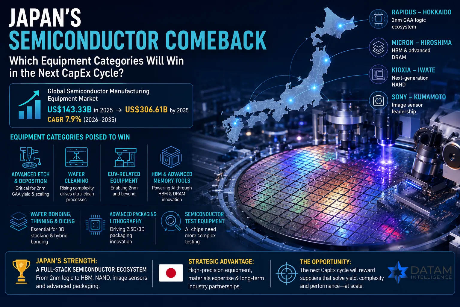
DataM Intelligence estimates that the global semiconductor manufacturing equipment market was worth US$143.33 billion in 2025 and could reach US$306.61 billion by 2035, expanding at a CAGR of 7.9%.
For Japan, however, the opportunity should not be reduced to capturing a percentage of a growing global equipment market.
Japan is simultaneously building a 2nm logic ecosystem in Hokkaido, advanced DRAM and HBM capabilities in Hiroshima, next-generation NAND capacity in Iwate, image-sensor capacity in Kumamoto, and a stronger domestic advanced-packaging ecosystem.
That creates very different equipment requirements.
And it means the most valuable categories during the next Japanese semiconductor CapEx cycle may not be the obvious ones.
Request Sample on Semiconductor Manufacturing Equipment Market
Which Semiconductor Equipment Categories Look Strongest in Japan?
The short answer is:
Advanced etch and deposition, wafer cleaning, EUV-related process equipment, HBM and advanced-memory tools, wafer bonding, precision thinning and dicing, advanced packaging lithography, and semiconductor test equipment appear best positioned.
This conclusion becomes clearer when Japan's actual fab programs are examined individually rather than treating semiconductor equipment as one homogeneous market.
SEMI's July 2026 outlook reinforces that change. Global semiconductor equipment sales are forecast to reach a record US$165.9 billion in 2026, up 23.2% year over year. Wafer fab equipment alone is expected to reach US$143.9 billion, while semiconductor test equipment is projected to rise 31% to US$15.3 billion. The strongest spending is being linked to advanced logic, HBM-related DRAM, memory and increasingly complex packaging.
Japan is unusually well exposed to several of those categories.
1. Rapidus Is Creating a 2nm Equipment Laboratory in Hokkaido
Chitose, Hokkaido is no longer simply another announced semiconductor fab location.
Rapidus's IIM manufacturing hub has had its pilot line operating since April 2025 and is targeting 2nm GAA semiconductor mass production from 2027. The facility already contains Japan's first volume-production-ready EUV lithography system, an ASML NXE:3800E installed in December 2024.
What matters for equipment suppliers in 2026 is what happens after installation.
METI's latest Rapidus program shows that the project has moved into yield improvement, defect-density reduction, equipment validation and short-turnaround-time manufacturing-system verification.
For fiscal 2026, the approved government-supported program includes up to ¥514.1 billion for front-end development and ¥117.4 billion for advanced back-end work. The latter includes verification of 2.xD and 3D packaging processes and the start of a multilayer RDL interposer development line.
That distinction is important.
Once a pilot fab starts chasing yield rather than simply installing equipment, purchasing decisions increasingly shift toward tools that can solve process variation.
That makes etch, deposition, cleaning, metrology, inspection and process-control equipment strategically valuable.
The real Rapidus equipment opportunity is therefore not one EUV scanner.
It is the ecosystem of equipment required to make 2nm wafers commercially repeatable.
2. HBM Is Turning Hiroshima Into an Equipment Demand Center
Japan's memory equipment opportunity is also changing.
On July 4, 2026, Micron broke ground on a new cleanroom at its Hiroshima operation to support advanced memory for AI. The Hiroshima facility has already played a role in 1-beta DRAM manufacturing and the adoption of EUV technology for 1-gamma DRAM, while Micron says its Japanese team is contributing to next-generation DRAM and HBM development.
METI had previously approved support of up to roughly ¥500 billion for Micron's investment program.
This has implications far beyond lithography.
HBM requires demanding DRAM front-end processes, but value increasingly accumulates after the wafer is fabricated.
Memory dies must be thinned, inspected, stacked, bonded, interconnected and tested while maintaining extremely high yields.
That brings Japanese suppliers such as Tokyo Electron, Advantest, DISCO and SCREEN into different parts of the same AI memory investment cycle.
The equipment opportunity is effectively spreading from the cleanroom into packaging.
3. Test Equipment Could Capture More Value Than Many Expect
Testing used to be easier to describe as a back-end necessity.
AI has changed that.
Advantest's July 2026 results described a structural shift in semiconductor testing as AI chips become more complex. The company reported record quarterly sales and said increasing AI semiconductor production was generating strong investment in its test systems.
Its commentary is particularly significant because inference AI is broadening demand beyond a narrow group of GPUs into ASICs, CPUs and DRAM.
More complex packaging, high-speed I/O, thermal behavior and power management are also increasing the number and difficulty of test requirements. Advantest expects the tester market to reach a record level and is expanding production capacity to meet demand.
That changes the economics of semiconductor equipment.
When a chip contains multiple expensive dies inside a sophisticated package, discovering that one component is defective after final assembly becomes extremely costly.
Manufacturers therefore have a financial incentive to identify Known Good Dies before packaging.
Tokyo Electron responded directly to this issue in April 2026 with its new Prexa SDP device prober for testing singulated devices used in advanced 2.5D and 3D semiconductor packages.
For Japan, test is therefore becoming part of yield economics rather than simply an end-of-line quality check.
That could make probers, handlers, SoC testers, memory testers and device-interface technologies some of the strongest-value equipment categories of the AI cycle.
4. Wafer Thinning and Dicing Are Becoming AI Infrastructure Technologies
Another overlooked category is precision wafer processing.
AI chips and HBM packages increasingly need thinner dies, more complicated stacking and tighter dimensional control.
DISCO provides a useful signal.
In March 2026, the Japanese equipment manufacturer announced that cumulative shipments of its laser saw systems had exceeded 4,000 units. Importantly, DISCO said the rate at which it shipped its latest 2,000 systems was almost three times the pace of the previous 2,000.
The company directly connected expanding laser-processing applications with advanced logic, HBM, ultra-thinned memory, SiC and next-generation semiconductor materials.
This is a good example of why the AI semiconductor equipment cycle should not be analysed only through lithography spending.
As architectures become three-dimensional, the wafer increasingly has to be ground, thinned, cut and prepared for stacking with extraordinary precision.
Those steps occur later in manufacturing but can determine the yield of an extremely expensive package.
In other words, AI may increase the economic importance of the tools that physically shape the chip after its transistors have already been fabricated.
5. Advanced Packaging Is Becoming a Japanese Equipment Battlefield
Japan historically maintained deep strength in semiconductor materials and front-end equipment, but advanced packaging now offers an opportunity to reconnect several areas of domestic engineering expertise.
Tokyo Electron's technology roadmap shows opportunities across wafer bonding, laser processing, temporary bonding and debonding, HBM metal etching, coating/development and advanced device testing.
SCREEN is also repositioning.
The company acquired Nikon's wafer-bonding R&D business in 2025, combining Nikon's high-precision bonding capabilities with SCREEN's packaging technology. SCREEN explicitly identified advanced packaging as a high-growth field.
Nikon, meanwhile, announced in June 2026 that it is developing a new 1.5 µm-resolution digital lithography system specifically for advanced semiconductor packaging, targeting more than 30% higher throughput than its existing DSP-100 platform. Commercial release is planned for fiscal 2027.
Rapidus adds another important element.
Its Chiplet Solutions program has already been working on 600 mm-square organic RDL interposer technology, along with 3D packaging and advanced back-end process development.
This may become one of Japan's most strategically important equipment opportunities.
The industry is moving from selling machines for making an individual silicon die toward supplying systems that help combine many dies into one compute system.
That expands the addressable equipment stack.
6. Cleaning Equipment May Be Quietly Becoming More Valuable
Cleaning rarely receives the attention given to lithography.
But advanced devices contain more process steps, more surfaces, more temporary bonding and more opportunities for contamination to destroy yield.
SCREEN's strategy provides evidence of where this is going.
The company expects leading-edge investment centered on HBM to remain important and has expanded R&D beyond cleaning into annealing and advanced packaging. It has also integrated wafer-bonding capabilities and is collaborating with Applied Materials through the EPIC Center to combine SCREEN's wafer-cleaning and surface-preparation expertise with materials engineering.
For 2nm, 3D NAND and stacked-memory manufacturing, surface preparation is not simply factory housekeeping.
Every additional interface between materials creates another point where particles, residues or surface variation can affect yield.
That makes cleaning equipment a yield-protection tool.
And yield protection becomes more valuable as the wafer becomes more expensive.
7. Kioxia Keeps Japan Relevant in the 3D NAND Equipment Cycle
Japan's equipment opportunity is not dependent entirely on 2nm and HBM.
Kioxia and Sandisk began production of their 10th-generation 3D flash memory at Fab2 of the Kitakami Plant in Iwate in July 2026. The companies said continued investment in the facility would support long-term NAND production and AI-related storage requirements.
Increasing the vertical density of 3D NAND changes equipment requirements dramatically.
Deep channel structures make high-aspect-ratio etching harder. More layers increase deposition requirements. Surface preparation becomes more demanding. Process variation becomes harder to tolerate.
Tokyo Electron's own technology roadmap highlights slit etch, channel-hole etch, molybdenum deposition, batch cleaning, wafer bonding and laser tools among the opportunities associated with future high-layer-count NAND.
Japan therefore has three separate AI-related memory equipment drivers:
HBM for bandwidth, advanced DRAM for AI compute, and NAND for the storage requirements created by AI inference.
That makes the Japanese memory-equipment story broader than HBM alone.
Kumamoto Has Exposed Another Equipment Requirement: Resilience
There is one factor semiconductor-equipment forecasts rarely price properly: where the tools are manufactured and serviced.
The July 28, 2026 Kumamoto earthquake offered a reminder.
Tokyo Electron temporarily suspended operations at its Koshi and Ozu sites to conduct safety inspections. Those facilities develop and manufacture coater/developers, cleaning systems and 3D packaging equipment. TEL subsequently said there was no significant damage and expected the business impact to be insignificant.
The disruption was limited, but the strategic message is larger.
Kumamoto is becoming increasingly important to Japan's semiconductor ecosystem. Sony and TSMC announced in August 2026 a new joint venture in Koshi City for next-generation image sensors, with Sony planning to contribute roughly ¥465 billion and TSMC roughly ¥282 billion. Volume production is targeted for 2029.
As clusters become denser, equipment procurement will increasingly include questions about spare-parts availability, local field engineers, seismic resilience, supplier redundancy and recovery time.
After-sales infrastructure may become a competitive advantage almost as important as equipment specifications.
Where Should Semiconductor Equipment Companies Focus in Japan?
The strongest opportunity is unlikely to come from chasing every fab expansion equally.
For suppliers targeting Japan, the next CapEx cycle can be divided into four commercial zones.
Hokkaido: 2nm GAA, EUV-related processing, deposition, etch, inspection, metrology, automation and advanced packaging around Rapidus.
Hiroshima: advanced DRAM, EUV process migration, HBM and AI memory equipment around Micron.
Iwate and Yokkaichi: 3D NAND scaling, high-aspect-ratio processing, deposition, cleaning and memory production around Kioxia.
Kumamoto: foundry manufacturing, image sensors, coating/development, cleaning, packaging and increasingly dense equipment-service infrastructure.
The sales strategy should also change.
Winning Japanese semiconductor equipment business will increasingly require suppliers to arrive before the purchase order-during process-development, pilot-line, yield-learning and qualification stages.
Once equipment becomes part of a customer's process-of-record, displacement becomes substantially harder.
That makes joint development, local application engineering and rapid service response powerful commercial tools.
The Bigger Opportunity: Sell Yield, Not Equipment
Japan's semiconductor revival should not be measured only by how many fabs are constructed.
The deeper opportunity lies in how difficult the next generation of chips will be to manufacture.
A 2nm GAA processor needs more process control than a mature-node chip. HBM needs more precision packaging than conventional DRAM. High-layer-count NAND increases etch and deposition difficulty. Chiplets create more bonding and testing requirements.
Every layer of complexity creates another point at which equipment can protect yield.
That is why the next winners in Japan may not simply be companies selling the most expensive machines.
They will be companies capable of proving that their equipment can reduce defects, shorten qualification, increase throughput, prevent downstream package losses and keep increasingly expensive wafers productive.
The global semiconductor manufacturing equipment market may be heading toward US$306.61 billion by 2035, but Japan's most important opportunity is more specific.
The country is rebuilding an ecosystem where Tokyo Electron, Advantest, SCREEN, DISCO, Canon, Nikon and other Japanese technology suppliers can participate in several value layers at once-from front-end wafer processing to advanced packaging and final test.
The next semiconductor CapEx cycle will therefore not be won by asking simply:
“How many new fabs will be built?”
The more useful question for Japan is:
“Which new process step becomes difficult enough that semiconductor manufacturers cannot scale without buying a better tool?”
Right now, the evidence points toward advanced etch and deposition, cleaning, HBM processing, wafer bonding, precision thinning and dicing, advanced packaging lithography, probing, and semiconductor test.
Those are the places where Japan's next semiconductor equipment battle is already taking shape.
Read the complete research report: https://www.datamintelligence.com/research-report/semiconductor-manufacturing-equipment-market