


According to DataM Intelligence, the global semiconductor manufacturing equipment market reached USD 143.33 billion in 2025 and is expected to reach USD 306.61 billion by 2035, expanding at a CAGR of 7.90% during 2026–2035. The opportunity is being created not only by new fabrication plants, but also by the growing number of manufacturing steps required for advanced logic, high-bandwidth memory, three-dimensional NAND, power devices and heterogeneous semiconductor packages.
Artificial intelligence is accelerating this transition. Training and inference infrastructure require processors with higher transistor density, faster memory access and more efficient communication between logic and memory. Producing these devices requires improvements across lithography, deposition, etching, cleaning, metrology, inspection, wafer bonding and semiconductor testing.
The result is a wider equipment investment cycle. A new generation of AI chips cannot be manufactured simply by installing more of the same tools. It requires new process capabilities, tighter tolerances, additional inspection points and deeper coordination between front-end wafer fabrication and advanced packaging.
For the United States, the opportunity centres on rebuilding production capacity, strengthening domestic equipment and material supply chains, and expanding leading-edge logic, memory and packaging infrastructure. For Japan, the opportunity builds on long-established strengths in semiconductor production equipment, materials, precision components, cleaning, testing and process control, supported by renewed investment in advanced logic and chiplet manufacturing.
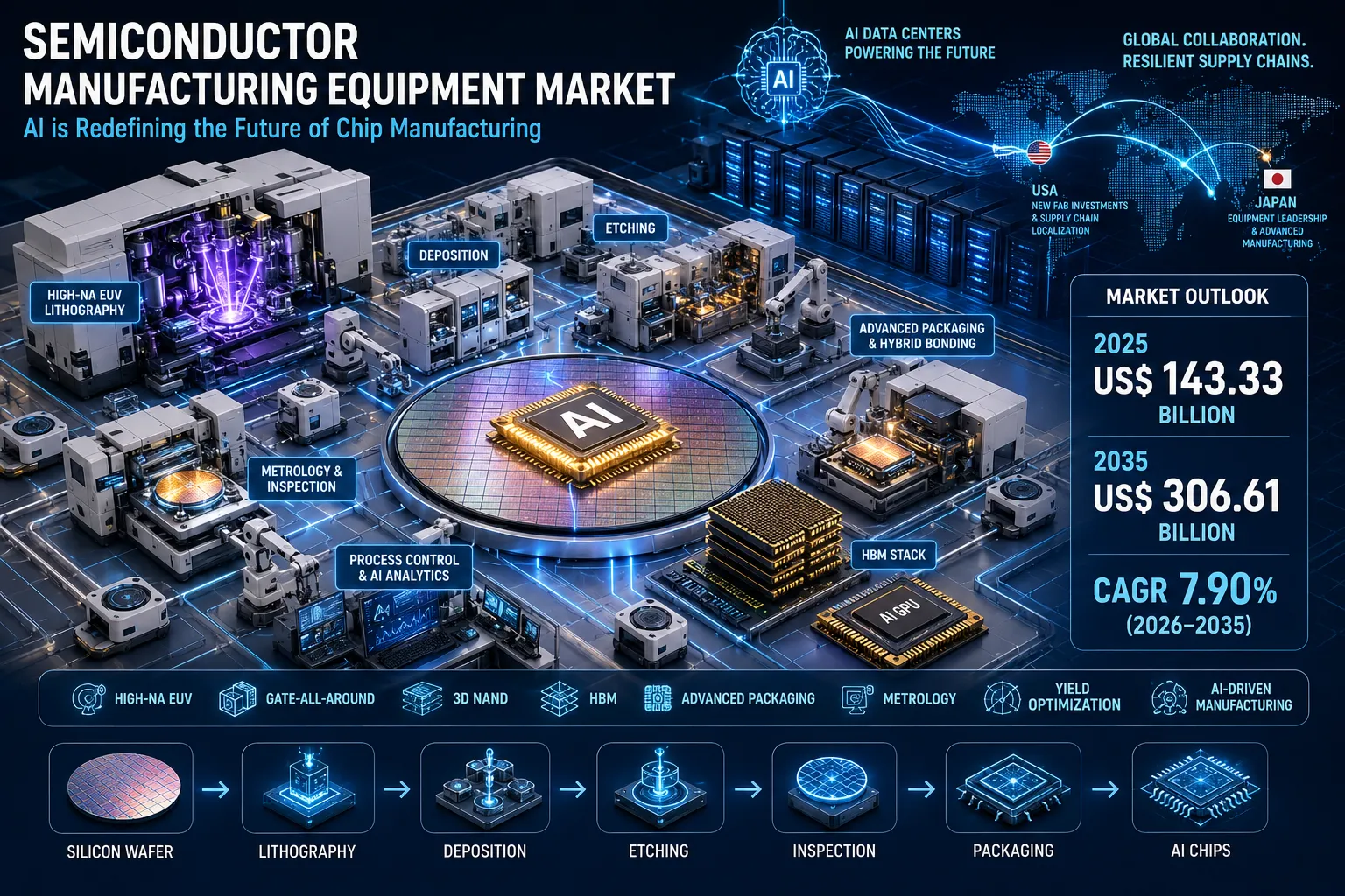
Request For Exclusive Sample On Semiconductor Equipment Manufacturing Market
Key Takeaways
- The semiconductor manufacturing equipment market is expected to more than double between 2025 and 2035.
- AI is increasing equipment demand across logic, DRAM, HBM and advanced packaging.
- High-NA EUV is an important technology transition, but conventional EUV and DUV will remain essential.
- Etch, deposition, cleaning and process control are gaining importance as semiconductor structures become more three-dimensional.
- HBM is connecting front-end memory production with wafer thinning, bonding, packaging, inspection and testing.
- The United States is investing in fabs and domestic supply-chain capacity, while Japan is reinforcing its equipment, materials and advanced-manufacturing ecosystem.
- Yield, uptime, service coverage and qualification speed can matter more than the initial price of a manufacturing tool.
Semiconductor Equipment Has Become a Strategic Capacity Engine
Semiconductor manufacturing equipment was once discussed primarily in relation to wafer starts and periodic capacity cycles. That view is now incomplete.
At advanced nodes, capacity is determined by more than cleanroom space and installed wafer volume. It depends on whether each tool can deliver the required process precision, throughput, uniformity and availability.
Modern semiconductor production can involve hundreds or thousands of tightly controlled steps. A failure in one deposition, etch, cleaning or inspection process can affect the performance of every subsequent layer.
The growing complexity creates three distinct equipment opportunities:
- Capacity equipment that increases the number of wafers or packages a facility can process.
- Technology-enabling equipment that supports new transistor structures, materials and packaging architectures.
- Productivity equipment and software that increase yield, improve availability and reduce production variability.
This distinction is important. A facility may have adequate theoretical wafer capacity but still be unable to meet output targets because of low yield, insufficient inspection, long cycle times or process bottlenecks.
The commercial value of an equipment platform should therefore be measured by its effect on saleable semiconductor output-not only its stated wafers-per-hour specification.
2026 Official Developments Reshaping Semiconductor Manufacturing Equipment
Several developments during 2026 demonstrate how rapidly the semiconductor equipment landscape is moving.
High-NA EUV moves closer to production deployment
ASML reported in April 2026 that it had shipped eight High-NA systems by the end of 2025 and that six were operating, including its first second-generation TWINSCAN EXE:5200B installation. The company said it was working toward meeting high-volume manufacturing requirements by the end of 2026, with customer insertion expected during 2027–2028.
High-NA EUV is more than a replacement cycle for lithography scanners. Its introduction affects photoresists, masks, pellicles, computational lithography, overlay control, defect inspection and fab-layout planning.
Equipment innovation expands around HBM and 3D architectures
In June 2026, Applied Materials introduced semiconductor systems targeting advanced DRAM and packaging for AI chips. The portfolio included equipment for DRAM epitaxy, chemical mechanical planarization, deposition and electron-beam inspection, with applications in chip stacking, HBM and three-dimensional semiconductor architectures.
The announcement shows why HBM demand is relevant to a much broader supplier base. It creates opportunities not only in DRAM wafer fabrication, but also in thinning, bonding, interconnect formation, planarization, defect review and package-level inspection.
Semiconductor development becomes more collaborative
Applied Materials and Micron announced a 2026 partnership involving joint research in advanced DRAM, HBM and NAND technologies. Meanwhile, IBM and Lam Research announced a collaboration covering materials and process technologies for sub-1nm logic scaling.
These partnerships reflect an important shift. Equipment innovation is increasingly being developed alongside device architectures rather than after a chip design has been completed.
Japan accelerates its 2nm manufacturing programme
Rapidus secured substantial government and private funding during 2026 as it prepared to move from research and development toward full-scale 2nm logic manufacturing. Its fiscal 2026 plans also cover 2nm integration, short-turnaround manufacturing and chiplet packaging technologies.
Japan’s Ministry of Economy, Trade and Industry also updated its Semiconductor and Digital Industry Strategy in June 2026. The strategy connects semiconductor manufacturing with AI models, computing infrastructure, communications, electricity, cybersecurity and workforce development, positioning chip production as part of a larger industrial ecosystem.
Equipment data confirm the strength of the investment cycle
SEMI projected worldwide 300mm fab equipment spending to rise by 18% to USD 133 billion in 2026 and by another 14% to USD 151 billion in 2027. The association linked the expansion to AI chip demand, advanced-node production and regional supply-chain investment.
These figures should not be directly compared with the DataM Intelligence total market forecast because the underlying scope and methodology differ. Together, however, they demonstrate the scale of near-term spending and the longer-term structural opportunity.
Understanding the Semiconductor Manufacturing Equipment Value Chain
Semiconductor production equipment can be divided into front-end, back-end and supporting systems.
Front-end wafer-fabrication equipment
Front-end manufacturing forms the circuits and device structures on a semiconductor wafer.
Major equipment categories include:
- Lithography systems
- Etching equipment
- Chemical and physical vapour deposition systems
- Atomic-layer deposition equipment
- Ion implantation systems
- Oxidation and thermal-processing equipment
- Chemical mechanical planarization systems
- Wafer cleaning equipment
- Metrology and inspection systems
Front-end equipment represents the largest strategic area of semiconductor fabrication expenditure because it directly determines transistor structures, feature dimensions and wafer-level yield. DataM Intelligence identifies front-end equipment as the principal equipment segment, supported by advanced logic, memory, power-device and sensor production.
Back-end and advanced-packaging equipment
Back-end equipment supports the transformation of processed wafers into tested semiconductor devices and integrated packages.
The category includes:
- Wafer thinning and grinding
- Wafer and die dicing
- Die placement
- Thermal compression bonding
- Hybrid bonding
- Through-silicon-via processing
- Redistribution-layer formation
- Moulding and encapsulation
- Package inspection
- Burn-in and electrical testing
The distinction between front-end and back-end manufacturing is becoming less rigid. Advanced packages now combine logic, memory, substrates, interposers and chiplets in configurations that directly determine system performance.
Supporting fab infrastructure
A semiconductor facility also requires systems that do not directly form the transistor but remain essential to production.
These include:
- Automated wafer handling
- Vacuum and pumping systems
- Specialty gas and chemical delivery
- Process-abatement equipment
- Cleanroom contamination control
- Factory scheduling software
- Equipment monitoring
- Predictive maintenance
- Manufacturing execution systems
- Advanced process control
A successful equipment investment plan must evaluate this complete ecosystem. Installing a critical process tool without adequate utilities, automation, inspection or service infrastructure can delay qualification and reduce productive capacity.
Where Semiconductor Equipment Creates Value
| Equipment category | Manufacturing role | Principal demand driver | Critical evaluation metric |
| Lithography | Transfers circuit patterns to wafers | Advanced logic and memory scaling | Resolution, overlay and throughput |
| Etching | Removes selected materials | GAA, 3D NAND and complex vertical structures | Selectivity, uniformity and profile control |
| Deposition | Forms thin material layers | New materials and three-dimensional devices | Film quality and thickness control |
| CMP | Planarizes wafer surfaces | Multilayer devices and advanced packaging | Uniformity and defect performance |
| Cleaning | Removes particles and residues | Higher process-step counts | Contamination control and chemical efficiency |
| Metrology | Measures dimensions and material properties | Tighter process tolerances | Accuracy and measurement speed |
| Inspection | Detects defects | Advanced nodes, HBM and packaging | Sensitivity and false-positive control |
| Bonding | Integrates wafers or dies | HBM, chiplets and 3D integration | Alignment accuracy and bond quality |
| Testing | Validates device performance | Complex, high-power semiconductors | Test coverage and throughput |
Request For Exclusive Sample On Semiconductor Equipment Manufacturing Market
Why AI Is Increasing Equipment Intensity
Artificial intelligence affects semiconductor equipment demand through four connected areas.
Leading-edge logic
AI accelerators require high computing density and improved power efficiency. These requirements are driving adoption of advanced transistor structures, including gate-all-around and nanosheet architectures.
Such structures require extremely selective etching, conformal deposition and precise process control. A small deviation in film thickness, critical dimension or material removal can reduce device performance or wafer yield.
High-bandwidth memory
AI systems need rapid movement of data between processors and memory. HBM addresses this requirement by stacking memory dies and connecting them through high-density interconnects.
Its production requires investments across:
- Advanced DRAM processes
- Through-silicon vias
- Wafer thinning
- Die stacking
- Precision bonding
- Package inspection
- Thermal management
- High-speed testing
SEMI projected global 300mm memory-equipment investment to exceed USD 50 billion in 2026, including an expected 29% increase in DRAM equipment spending to USD 37 billion, supported by demand for HBM and DDR5 memory.
Advanced packaging
Traditional performance improvement depended heavily on shrinking transistor dimensions. The industry is now also improving performance by integrating specialised dies in one package.
This creates demand for equipment supporting:
- Chiplet architectures
- 2.5D integration
- 3D integrated circuits
- Hybrid bonding
- Fan-out packaging
- Glass and silicon interposers
- Fine-pitch redistribution layers
KLA has highlighted that advanced packaging increases manufacturing complexity by combining compute and memory devices, making process control and package-level yield management more important.
Yield and productivity
An advanced chip may pass through a large number of expensive process steps before a defect becomes visible. Discovering a problem late in production can therefore destroy much more value than detecting it immediately.
This is increasing demand for:
- Inline inspection
- Virtual metrology
- Automated defect classification
- Equipment health monitoring
- Predictive process control
- Root-cause analytics
The economic objective is not simply to identify defective wafers. It is to shorten the time required to understand why defects occur and correct the process before additional production is affected.
High-NA EUV Will Expand the Equipment Ecosystem
Lithography remains one of the most visible semiconductor equipment categories, but the future is not a simple transition in which one generation replaces all previous systems.
DUV lithography
Deep ultraviolet systems will continue to support mature nodes, non-critical layers and many logic and memory applications. They remain productive, established and widely integrated across the global fab base.
Conventional EUV
EUV systems reduce some of the complex multi-patterning steps that would otherwise be required at advanced nodes. They are expected to remain central to leading-edge production even as High-NA systems are introduced.
High-NA EUV
High-NA EUV increases numerical aperture to improve resolution for future semiconductor nodes. ASML describes its EXE platform as capable of supporting smaller features than existing NXE systems.
Its commercial importance extends beyond the scanner.
High-NA adoption can create demand for:
- New photoresist processes
- Reticle inspection
- Mask infrastructure
- Track systems
- Overlay metrology
- Computational pattern correction
- Defect review
- Vibration control
- Facility modifications
- Operator training
The investment decision will depend on more than technical capability. Each manufacturer must evaluate process simplification, tool productivity, expected wafer volume, qualification timelines and the value of gaining earlier access to future nodes.
Etch and Deposition Are Becoming More Important
Semiconductor scaling is increasingly a materials-engineering challenge.
Gate-all-around transistors, 3D NAND and advanced DRAM require structures that are narrower, taller and more difficult to manufacture. The industry must deposit materials uniformly on complex surfaces and selectively remove specific layers without damaging adjacent structures.
This increases demand for:
- Atomic-layer deposition
- Selective deposition
- High-aspect-ratio etching
- Atomic-layer etching
- Plasma-process control
- Advanced wafer cleaning
- Uniformity measurement
In 3D NAND, additional memory layers increase etch depth and deposition complexity. In advanced logic, new channel, gate and interconnect materials require tighter control over film composition and interface quality.
These developments mean that node advancement cannot be evaluated only by the number of lithography steps. The number and difficulty of deposition, etch, cleaning and measurement processes are equally important.
HBM Is Creating a New Equipment Investment Cycle
High-bandwidth memory represents one of the clearest examples of front-end and back-end manufacturing converging.
HBM begins with advanced DRAM wafers, but performance depends on how accurately individual dies are thinned, aligned, connected and tested.
A simplified HBM equipment flow includes:
- DRAM wafer fabrication
- Through-silicon-via formation
- Wafer thinning
- Die separation
- Die inspection
- Precision stacking
- Bonding
- Encapsulation
- Package-level inspection
- Electrical and thermal testing
Yield becomes especially important because one defective die can affect an entire stacked product. As stack heights and interconnect density rise, equipment must control warpage, alignment, bonding quality and thermal stress.
This makes advanced inspection and testing central to the HBM investment case. The industry needs to identify defects before expensive dies are incorporated into larger packages.
Why Metrology and Inspection Are Strategic Investments
Metrology measures process characteristics. Inspection identifies physical defects. Both are becoming more important as manufacturing tolerances narrow.
At advanced nodes, manufacturers need to control:
- Critical dimensions
- Overlay accuracy
- Film thickness
- Material composition
- Pattern shape
- Surface defects
- Wafer stress
- Package warpage
- Bond alignment
- Interconnect quality
KLA’s portfolio illustrates how inspection, metrology and analytics are used across semiconductor fabrication to improve yield and accelerate production ramps.
The return on process-control equipment should be considered in relation to the cost of delayed yield learning. A new fab may contain billions of dollars in installed capacity, but that capacity does not become economically productive until the facility can manufacture acceptable devices consistently.
Faster defect detection can therefore improve:
- Time to qualification
- Yield-ramp speed
- Tool utilisation
- Customer delivery
- Capital productivity
- Gross margin
Equipment Economics Must Extend Beyond Purchase Price
The initial purchase price of a semiconductor tool represents only one component of its total economic impact.
Capital requirements
A complete investment assessment should include:
- Tool acquisition
- Transportation and installation
- Cleanroom preparation
- Gas, chemical, power and water connections
- Vibration and temperature controls
- Process qualification
- Automation integration
- Initial spare parts
- Training
Operating requirements
Operating expenses include:
- Energy consumption
- Water use
- Specialty gases
- Process chemicals
- Consumables
- Preventive maintenance
- Replacement parts
- Software support
- Service contracts
- Waste treatment
Productivity considerations
Critical performance indicators include:
- Wafers per hour
- Overall equipment effectiveness
- Mean time between failures
- Mean time to repair
- Process repeatability
- Defect density
- Yield
- Utilisation
- Qualification time
- Upgrade potential
A lower-priced tool can become the more expensive choice when it causes additional downtime, lower yield or longer process qualification.
The most useful commercial measure is the cost per saleable wafer or package over the equipment’s productive life.
United States Semiconductor Equipment Outlook
The United States is attempting to rebuild a more complete semiconductor manufacturing ecosystem. The opportunity includes advanced logic, memory, power devices, photonics, packaging, materials and equipment production.
CHIPS for America was established with USD 50 billion for semiconductor research, development and manufacturing programmes. The initiative includes support for domestic semiconductor production and the wider supply chain required to operate fabs.
An amended funding opportunity also covers the construction, expansion or modernisation of commercial facilities producing semiconductor materials and manufacturing equipment. This is significant because domestic fabs remain dependent on reliable access to tools, components, chemicals, gases and technical services.
Why new fabs create multiyear equipment demand
A fab announcement does not translate immediately into tool revenue or production output.
Projects progress through:
- Site preparation
- Building construction
- Cleanroom completion
- Utility installation
- Equipment move-in
- Process qualification
- Yield ramp
- Volume production
Equipment orders may be placed well before commercial output begins. Suppliers must align manufacturing capacity and service resources with these timelines.
Advanced packaging is a strategic gap
Producing leading-edge wafers domestically is only one part of supply-chain resilience. AI processors may still depend on overseas capacity for interposers, HBM integration, substrate production, assembly and testing.
This creates an opportunity for U.S. investment in:
- Chiplet integration
- Hybrid bonding
- HBM packaging
- Package inspection
- Substrate manufacturing
- Thermal testing
- Reliability qualification
Installation and service capacity matter
A new concentration of fabs increases demand for equipment engineers, maintenance specialists, applications support and spare-parts logistics.
Tool availability without sufficient field-service capacity can lengthen downtime and delay technology ramps. The ability to support multiple facilities near major manufacturing clusters will become an important supplier differentiator.
Utilities remain a critical constraint
Semiconductor fabs require reliable electricity, high-purity water, specialty gases and advanced waste-management infrastructure.
Equipment selection will increasingly be evaluated alongside utility efficiency. Systems that reduce chemical consumption, energy demand or process waste may deliver strategic value in regions where permitting and infrastructure are constrained.
Japan Semiconductor Equipment Outlook
Japan enters the current investment cycle with different strengths.
Its semiconductor position extends beyond wafer fabrication to materials, photoresists, silicon wafers, cleaning systems, deposition, testing, precision components and equipment subsystems.
DataM Intelligence identifies Japan as an important equipment and materials base, supported by memory expansion, advanced manufacturing partnerships and government-backed semiconductor revitalisation.
Japan’s value lies in the complete manufacturing ecosystem
Japanese companies hold important positions in:
- Semiconductor production equipment
- Wafer cleaning
- Coater and developer systems
- Test equipment
- Silicon wafers
- Photoresists
- Specialty chemicals
- Precision motors and components
- Ceramic components
- Advanced substrates
This means Japan can benefit even when final wafer fabrication occurs in another country. Its suppliers are embedded throughout international production lines.
Advanced logic investment creates new domestic demand
Rapidus’ 2nm initiative can stimulate demand across lithography support, deposition, etch, cleaning, inspection, materials and advanced packaging.
The company’s 2026 programme includes 2nm integration and chiplet-related manufacturing, with a stated objective of progressing toward mass production in 2027.
Even if production targets evolve, the programme is strategically important because it creates a domestic environment for equipment qualification, materials development and advanced manufacturing collaboration.
Tokyo Electron reinforces Japan’s equipment position
Tokyo Electron operates across several critical semiconductor processes, including coating and developing, cleaning, etching, deposition and testing. Its portfolio is positioned around repeated patterning steps and advanced process requirements.
In 2026, the company also highlighted its use of artificial intelligence in semiconductor manufacturing solutions, reflecting the growing integration of equipment hardware, process knowledge and manufacturing software.
Japan can serve both advanced and specialised markets
Japan’s opportunity is not limited to leading-edge logic. Its manufacturing ecosystem also supports:
- NAND memory
- Image sensors
- Power semiconductors
- Automotive devices
- Radio-frequency components
- Photonics
- Sensors
- Advanced packaging
These markets require different equipment configurations and investment cycles, reducing dependence on one semiconductor segment.
USA and Japan: Complementary Equipment Opportunities
| Strategic factor | United States | Japan |
| Primary momentum | New fab construction and capacity localisation | Equipment, materials and advanced-manufacturing revitalisation |
| Major opportunity | Logic, memory, packaging and supplier localisation | Precision tools, cleaning, testing, materials and advanced logic |
| Existing strength | Process equipment, R&D and chip design | Production equipment, components and materials |
| Investment challenge | Construction costs, workforce and utilities | Manufacturing scale, workforce and commercial ramp speed |
| Supply-chain priority | Building a more complete domestic cluster | Reinforcing strategic global supplier positions |
| AI opportunity | Leading-edge logic and advanced packaging | Equipment innovation, HBM, materials and 2nm production |
Request For Exclusive Sample On Semiconductor Equipment Manufacturing Market
The United States offers a large pipeline of new capacity and technology development. Japan offers equipment, material and precision-manufacturing capabilities that can support those projects. Partnerships between research organisations, device manufacturers and equipment suppliers can therefore strengthen both ecosystems.
AI Is Also Transforming Semiconductor Manufacturing Operations
The industry is experiencing two simultaneous trends:
- Equipment is being purchased to manufacture AI chips.
- AI is being incorporated into manufacturing equipment and fab operations.
AI-enabled semiconductor manufacturing applications include:
- Predictive maintenance
- Equipment-failure detection
- Defect classification
- Virtual metrology
- Process-recipe optimisation
- Yield prediction
- Automated root-cause analysis
- Production scheduling
- Energy optimisation
- Tool matching
- Digital twins
Process data can reveal patterns that are difficult to detect using traditional statistical methods. For example, a model may identify relationships between chamber conditions, material variations and downstream defects.
However, semiconductor manufacturing requires controlled deployment. A process recommendation must be explainable, validated and compatible with strict change-management procedures. An inaccurate adjustment can affect a large quantity of high-value wafers.
The strongest use cases will therefore combine AI with process-engineering knowledge rather than attempting to replace it.
Supply-Chain and Investment Risks
The industry’s growth outlook is substantial, but equipment programmes face several risks.
Supplier concentration
Some process technologies are supplied by a very small number of qualified vendors. A delay or production problem at one supplier can affect multiple fab projects.
Long qualification cycles
Switching equipment is rarely a simple procurement decision. A new platform may require recipe development, materials testing, reliability validation and customer approval.
Export-control uncertainty
Semiconductor equipment is increasingly affected by national-security and trade policies. Regulations can alter where certain systems, components, software updates and services may be supplied.
Because these rules change, every procurement programme should use current official government guidance rather than relying on historic assumptions.
Component and service availability
A tool may remain in production for many years. Buyers need confidence that spare parts, software support, field engineers and upgrade services will remain available throughout its useful life.
Workforce limitations
Advanced semiconductor equipment requires specialised installation, process and maintenance skills. Competition for experienced personnel can delay fab ramps and increase operating costs.
Utility and environmental constraints
Some tools require substantial power, water, gases and chemicals. Local infrastructure, environmental rules and waste-treatment capacity can affect equipment deployment.
A Practical Semiconductor Equipment Selection Framework
An effective selection process should evaluate the complete manufacturing and commercial requirement.
Process capability
- Can the system meet the required node or package specification?
- Does it provide adequate uniformity and repeatability?
- Can it support future device structures?
Productivity
- What is the proven production throughput?
- How quickly can the tool be qualified?
- What maintenance frequency is required?
- How does performance change at full utilisation?
Yield contribution
- Does the system reduce defects?
- Can it generate actionable process data?
- How easily can it integrate with existing process control?
Infrastructure compatibility
- What cleanroom space is required?
- What are its power, water, gas and exhaust requirements?
- Is it compatible with current automation and software?
Supplier readiness
- Is local service available?
- Are replacement parts stocked near the facility?
- Can the supplier support simultaneous fab ramps?
- Is there a clear technology-upgrade roadmap?
Total cost of ownership
- What is the cost per productive wafer or package?
- How does downtime affect output?
- What consumables and service costs are expected?
- Can the tool be upgraded rather than fully replaced?
Semiconductor Manufacturing Equipment Market Outlook Through 2035
DataM Intelligence expects the semiconductor manufacturing equipment market to increase from USD 143.33 billion in 2025 to USD 306.61 billion by 2035. Asia-Pacific remains both the largest and fastest-growing regional market because it concentrates foundry, memory, packaging and electronics-manufacturing capacity.
Front-end equipment will remain fundamental, but some of the most dynamic opportunities will emerge where process categories converge.
Leading opportunity areas
- High-NA EUV and its supporting ecosystem
- Gate-all-around transistor processes
- Atomic-layer deposition and etching
- High-aspect-ratio etching for 3D NAND
- Advanced DRAM and HBM equipment
- Hybrid and thermal-compression bonding
- Chiplet and heterogeneous integration
- Package-level inspection
- Semiconductor test equipment
- Yield-management software
- AI-enabled process control
- Equipment refurbishment and upgrades
- Resource-efficient fab systems
Major suppliers identified in the DataM Intelligence market landscape include ASML, Applied Materials, Tokyo Electron, Lam Research and KLA. Their positions span lithography, deposition, etch, cleaning, metrology, inspection and yield management.
The competitive advantage will increasingly come from solving integrated manufacturing problems.
A lithography platform creates more value when supported by effective resist processing and overlay control. An etch system creates more value when process variation can be measured immediately. A bonding platform creates more value when incoming dies have been inspected and package defects can be detected before final testing.
The market is therefore evolving from individual tool procurement toward coordinated manufacturing platforms.
Frequently Asked Questions
What is semiconductor manufacturing equipment?
Semiconductor manufacturing equipment includes the systems used to form, process, inspect, package and test semiconductor devices. Major categories include lithography, etching, deposition, cleaning, CMP, ion implantation, metrology, inspection, bonding and semiconductor test equipment.
What is the difference between front-end and back-end equipment?
Front-end equipment forms semiconductor structures on a wafer through processes such as lithography, deposition and etching. Back-end equipment separates, packages, connects and tests the completed dies. Advanced packaging is increasingly connecting the two stages because package architecture now directly affects semiconductor performance.
Why is AI increasing semiconductor equipment demand?
AI requires advanced processors, HBM and high-density packages. Manufacturing these devices involves more complex transistor structures, additional material layers, precision bonding and more inspection. AI therefore increases demand across both wafer-fabrication and advanced-packaging equipment.
What is High-NA EUV?
High-NA EUV is a new generation of extreme-ultraviolet lithography that uses a higher numerical aperture to print smaller semiconductor features. It is being developed for future advanced logic and memory nodes but requires supporting investments in masks, resists, metrology, inspection and fab infrastructure.
Will High-NA EUV replace conventional EUV and DUV?
It is unlikely to replace them completely. High-NA EUV will be used where its resolution and process benefits justify the investment. Conventional EUV and DUV will continue to support many critical, non-critical and mature-node layers.
What equipment is needed to manufacture HBM?
HBM manufacturing uses advanced DRAM fabrication equipment, through-silicon-via systems, wafer-thinning tools, dicing, die placement, bonding, inspection, encapsulation and high-speed test equipment. Yield control is essential because multiple memory dies are integrated into one product.
Why is advanced packaging important for AI chips?
Advanced packaging enables logic processors, HBM, chiplets and interposers to be integrated into one high-performance system. It improves bandwidth and system efficiency but introduces new challenges involving alignment, interconnect density, warpage, thermal management and package-level yield.
Which region leads the semiconductor manufacturing equipment market?
Asia-Pacific is the largest and fastest-growing region because it contains significant foundry, memory, packaging and electronics-manufacturing capacity in Taiwan, South Korea, China, Japan and Southeast Asia.
What factors determine semiconductor equipment ROI?
Important factors include purchase price, throughput, yield, uptime, maintenance, consumables, qualification time, process stability and upgrade potential. The most meaningful measurement is usually the lifetime cost per saleable wafer or packaged device.
What are the major semiconductor equipment opportunities in the USA and Japan?
The United States offers opportunities in new fab capacity, advanced packaging and domestic supply-chain development. Japan offers opportunities in production equipment, materials, precision components, testing, cleaning and advanced logic manufacturing.
Conclusion: Manufacturing Capability Will Decide the Next Phase of Semiconductor Growth
The semiconductor equipment market is no longer expanding solely because the world needs more chips. It is expanding because the chips required for artificial intelligence, high-performance computing, automotive systems, and industrial infrastructure are becoming considerably more difficult to manufacture.
High-NA EUV will push lithography forward, but progress will also depend on deposition, etching, cleaning, and process control. HBM will create demand for advanced memory tools, but its commercial success will also depend on thinning, bonding, inspection, and testing. New fabs will add capacity, but their economic value will depend on how quickly they achieve stable yield and productive utilisation.
The United States and Japan occupy strategically important-and complementary-positions partly in this transition. The United States is building new production, research and packaging capacity. Japan is reinforcing a manufacturing ecosystem built around equipment, materials, precision technologies and advanced semiconductor production.
Through 2035, the strongest opportunities will belong to technologies and suppliers that help semiconductor manufacturers achieve three outcomes simultaneously:
- Higher device performance
- Faster yield improvement
- More productive use of capital
As semiconductor architectures become more complex, equipment will not remain a supporting part of the industry. It will be one of the principal factors determining which technologies can move from laboratory development to reliable, profitable mass production.
Read Complete Research Report: https://www.datamintelligence.com/research-report/semiconductor-manufacturing-equipment-market