


Artificial intelligence is transforming demand for semiconductor manufacturing equipment. Each faster AI accelerator, higher-density memory device and more complex processor requires extraordinary precision during fabrication, assembly and testing. As chip designs become harder to manufacture, equipment suppliers are emerging as strategic partners in the global computing supply chain.
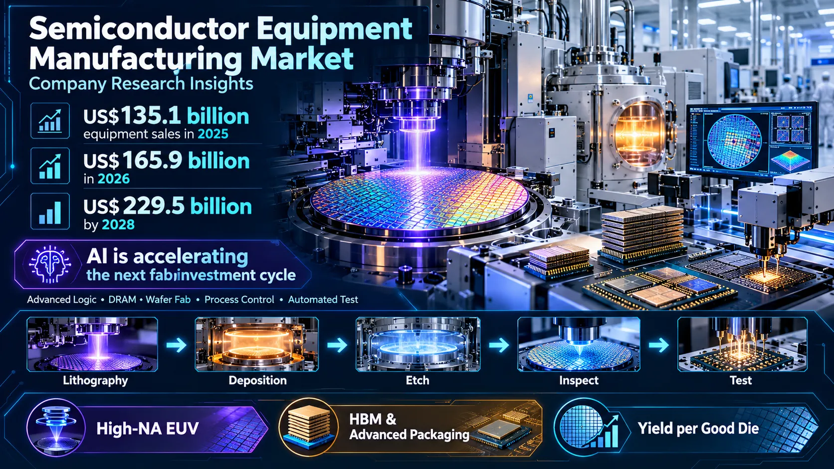
SEMI reported global semiconductor equipment billings of approximately $135 billion in 2025. Its July 2026 forecast projects original-equipment-manufacturer sales of $165.9 billion in 2026 and $229.5 billion in 2028. These are different reporting measures, but together indicate the scale of investment accelerating across the industry.
Request Sample: https://www.datamintelligence.com/download-sample/semiconductor-manufacturing-equipment-market
What Is Semiconductor Manufacturing Equipment?
Think of semiconductor manufacturing as printing an incredibly detailed electronic city onto a silicon wafer. The wafer passes through hundreds of controlled steps before it becomes the chips inside smartphones, vehicles, industrial machinery and AI servers. Semiconductor manufacturing equipment consists of the specialized machines that perform those steps.
Lithography tools project tiny circuit patterns onto wafers, rather like an ultra-precise photographic printer. Deposition systems build extremely thin material layers. Etching tools remove selected material to shape circuits, while cleaning equipment eliminates particles that could ruin a chip. Metrology and inspection systems check dimensions and defects. Finally, assembly, packaging and test tools connect individual chips, combine components and verify performance.
A “2 nm” process is an industry generation label rather than a literal measurement of every transistor feature. As manufacturers progress toward more complex architectures, even tiny production errors can destroy value. That makes precision, repeatability and production yield central to equipment purchasing decisions.
Where Are the Major Growth Opportunities?
1. AI Accelerators and Leading-Edge Logic
Chipmakers are investing in advanced logic manufacturing for GPUs, custom AI accelerators and high-performance processors. Gate-all-around transistor architectures and increasingly complex interconnects raise demand for deposition, etch, metrology and lithography capabilities. SEMI projects foundry-and-logic equipment sales of $78.0 billion in 2026.
2. High-Bandwidth Memory and 3D NAND
High-bandwidth memory (HBM) helps AI processors move large volumes of data rapidly. Building these memory stacks requires sophisticated wafer processing, thinning, bonding and inspection. SEMI forecasts DRAM equipment sales of $38.8 billion in 2026, reflecting substantial spending on HBM and advanced memory nodes. Taller 3D NAND architectures create additional etch and deposition challenges.
3. Advanced Packaging and Chiplets
Performance gains increasingly come from combining multiple chips in one package instead of relying on a single larger die. Hybrid bonding, wafer-level packaging, thermal management and precision assembly are therefore becoming major equipment opportunities. SEMI expects test equipment sales to reach $15.3 billion in 2026 while assembly and packaging equipment reaches $6.7 billion.
4. Regional Fab Investment and Supply-Chain Resilience
Government incentives and supply-security priorities are supporting new fabrication capacity in the United States, Europe, Japan and other locations. China, Taiwan and South Korea remain important equipment-spending centers. Expansion creates demand beyond new machines, including installation, qualification, localized service teams, spare parts and long-term maintenance.
5. Inspection, Yield Management and Equipment Services
At advanced nodes, a defective feature invisible to the naked eye can reduce output from an expensive production line. Inspection, process-control software and equipment upgrades help manufacturers improve yields. Recurring services may therefore become an increasingly attractive revenue stream alongside cyclical new-tool sales.
Where Is the Market Headed Through 2035?
Over the next decade, semiconductor equipment competition is likely to shift toward enabling more complex device architectures at commercially viable yields. High-NA EUV lithography, selective deposition, atomic-level etching, backside power delivery and advanced bonding could increase the value of each manufacturing step. Equipment suppliers will increasingly need to integrate hardware, sensors, process models and software.
Three structural changes stand out: more capital-intensive advanced fabs, faster growth in packaging and test complexity, and broader geographical diversification of manufacturing. However, equipment spending will remain cyclical, with potential delays from export controls, power and water limitations, qualification timelines and changing customer investment plans. The industry’s expansion through 2035 is a strategic outlook, not a straight-line continuation of near-term forecasts.
10 Major Companies Shaping the Market
- ASML - A leading supplier of advanced lithography systems, including EUV and high-NA EUV tools used to pattern cutting-edge chips.
- Applied Materials - A broad-based supplier of deposition, materials engineering, process control and advanced packaging equipment.
- Lam Research - A major provider of etch, deposition and wafer-cleaning systems for advanced logic and memory production.
- Tokyo Electron - Supplies deposition, coater/developer, etch and cleaning equipment across key wafer-fabrication steps.
- KLA - Specializes in inspection, metrology and process control used to improve semiconductor manufacturing yields.
- ASM International - Focuses on atomic layer deposition and related thin-film processes critical to advanced transistors.
- SCREEN Holdings - Supplies wafer-cleaning and surface-treatment equipment used at multiple chip manufacturing stages.
- Advantest - Provides semiconductor automatic test equipment, including systems for advanced processors and memory.
- Teradyne - Offers automated semiconductor test equipment for complex devices and high-volume production.
- DISCO Corporation - Specializes in high-precision wafer dicing, grinding and thinning used in advanced manufacturing and packaging.
Other participants include Nikon, Canon, Hitachi High-Tech, Onto Innovation, Nova, Axcelis Technologies, BE Semiconductor Industries (Besi), Kulicke & Soffa and ACM Research.
Competition increasingly centers on atomic-scale process precision, advanced packaging integration, defect detection, throughput, equipment uptime, software-led optimization and the ability to support customers across geographically diversified fab networks.
The Bigger Opportunity
The next semiconductor equipment cycle is about far more than building additional factories. Manufacturers need tools that make smaller transistors, stacked memory and multi-chip systems commercially reliable. Companies that solve these manufacturing bottlenecks will be positioned to capture value throughout the AI infrastructure expansion and the broader semiconductor technology roadmap.
Request Sample: https://www.datamintelligence.com/download-sample/semiconductor-manufacturing-equipment-market