Nanoscale Semiconductor Market Overview
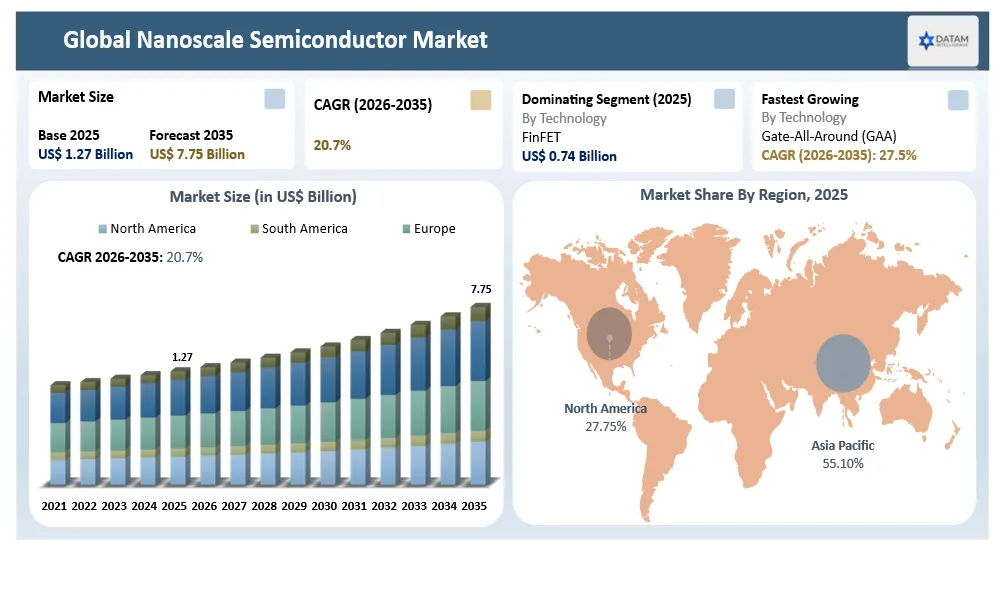
The global nanoscale semiconductor market reached US$ 1.27 billion in 2025 and is expected to reach US$ 7.75 billion by 2035, growing with a CAGR of 20.7% during the forecast period 2026-2035.
The industry is currently transitioning from FinFET architecture towards GAA nanosheet technology and commercializing 2nm technology. According to TSMC’s 2025 Annual Report, the revenue from the 3nm wafer accounted for 24%, whereas 7nm and below technologies increased the revenue to 74%, compared to 69% in 2024. The increase in this revenue from advanced nodes reveals an increase in the demand for increased transistor density, better performance per watt and power utilization for numerous applications such as AI accelerators, HPC processors, automotive and other computing applications.
According to TSMC, its 2nm N2 technology successfully entered high-volume manufacturing in Q4 2025 with good yield, marking an important commercial step in the transition to nanosheet-based transistor architectures. On the other hand, TSMC continues working on the N2P and A16 technologies, which will have volume production by H2 2026, while the A14 technology is based on the second generation of nanosheet transistors architecture. This is just an example that shows that competition in nanoscale semiconductors is moving away from transistor shrinkage and towards GAA architectures, advanced power delivery, EUV manufacturing, interconnects and advanced packaging.
Nanoscale Semiconductor Market Key Takeaways
- The FinFET held the maximum market share of 58% in the global nanoscale semiconductor market in 2025 supported by its deployment in 7nm, 5nm and 3nm class semiconductor devices used in CPUs, GPUs, mobile system-on-chips (SoC), AI chips and automotive processors.
- Gate All Around (GAA) is expected to be the highest growing technology segment at an estimated CAGR of 27.5%, due to its adoption for next-generation 2nm and sub-2nm semiconductors that increase the density of transistors, electrostatics control and performance per watt.
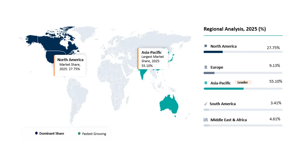
- Asia-Pacific captured the maximum market share of 55.10% in the global nanoscale semiconductor market in 2025 on account of presence of world-class foundries, advanced memory manufacturers, semiconductor wafer fabrication plants and packaging operations in Taiwan, South Korea, Japan and China.
- The 2nm process adoption is fastening the transition of chip architecture from FinFET to GAA architecture with TSMC's N2 going into high volume production during Q4 2025 and Samsung and Intel working on different competing GAA architectures.
- Deployment of AI accelerators, HPC processors, smartphone SoCs and cloud-server processors is driving semiconductor nanotechnology towards the direction of back-side power delivery, extreme ultraviolet patterning, chiplets, 2.5D and 3D packaging and high performance per watt.
Nanoscale Semiconductor Industry Trends and Strategic Insights
- GAA nanosheet technology is becoming the dominant scaling path beyond FinFET: Leading-edge logic will adopt GAA nanosheet devices at 3nm and 2nm class nodes to ensure improved gate control, transistor density and power efficiency.
- Forksheet and CFET are emerging as the next scaling architectures: The fork sheet technology will be used as an intermediate technology between GAA nanosheet devices and vertically-stacked CFET devices.
- Backside power delivery is becoming an important nanoscale scaling booster: Backside power delivery can help in solving front-side congestion issues and improving power delivery efficiency, thus gaining relevance in future AI and HPC processors.
- Atomic-scale process control is becoming strategically critical: As transistors scale down in size, deposition, selective etching, EUV lithography and metrology processes need to have ever greater control over the dimensions, interfaces and materials of nanosheets.
- The competitive focus is shifting from transistor scaling toward 3D system integration: The performance of future nanometer scale semiconductors will be more dependent upon the combination of advanced transistor structures with 3D integration and advanced interconnects.
Nanoscale Semiconductor Market Scope
| Metrics | Details | |
| 2025 Market Size | US$ 1.27 Billion | |
| 2035 Projected Market Size | US$ 7.75 Billion | |
| CAGR (2026-2035) | 20.7% | |
| Largest Market | Asia-Pacific | |
| Fastest Growing Market | Asia-Pacific | |
| By Technology | Transistor Architectures, Nanowire-Based Technologies and Quantum & Nanoelectric Devices | |
| By Process Node | Above 14nm, 10nm–14nm, 8nm, 7nm, 6nm, 5nm, 4nm, 3nm, 2nm and Below 2nm | |
| By Semiconductor Material | Silicon-Based Materials, Group IV / Silicon-Germanium Materials, III-V-Based Materials, Wide Bandgap Materials, Carbon-Based Materials, 2D Semiconductor Materials and Other Semiconductor Materials | |
| By Device Type | Logic Devices, Memory Devices, Sensors, Optoelectronic Devices, RF Devices, Quantum Devices and Other Nanoscale Devices | |
| By Wafer Size | Below 100 mm, 100 mm–149 mm, 150 mm–199 mm, 200 mm–299 mm, 300 mm–449 mm and 450 mm and Above | |
| By Application | Consumer Electronics, High-Performance Computing, Automotive, Telecommunications, Industrial Electronics, Healthcare & Medical Devices, Aerospace & Defense, Photonics, Energy & Power Electronics and Other Applications | |
| By End-User | Semiconductor Foundries, Integrated Device Manufacturers (IDMs), Fabless Semiconductor Companies, Electronics OEMs, Automotive OEMs, Data Center Operators, Telecommunications Companies, Research Institutions, Government & Defense Organizations and Other Industrial Users | |
| By Region | North America | U.S., Canada, Mexico |
| Europe | Germany, UK, Russia, France, Spain, Italy, Poland | |
| Asia-Pacific | China, India, Japan, Australia, South Korea, Indonesia, Malaysia, Singapore, Vietnam, Thailand, Philippines, Taiwan | |
| South America | Brazil, Argentina | |
| Middle East and Africa | UAE, Saudi Arabia, South Africa, Israel, Turkiye, Nigeria | |
| Report Insights Covered | Competitive Landscape Analysis, Company Profile Analysis, Market Size, Share, Growth | |
Why does this report matter in 2026?
The nanoscale semiconductor market is now at a crucial point of transition in 2026. This market is making a switch from FinFET to 2nm-class GAA/Nanosheet technology to increase density, reduce leakage and maximize performance per watt. It is vital for AI accelerators, high-performance computing, data centers and premium mobile processors as efficiency and performance have become very important in such segments.
This report will be highly relevant since scaling below 2nm is more dependent upon innovation in manufacturing processes than on shrinking nodes. High NA EUV, atomic-level deposition and etching, backside power delivery, advanced interconnects and novel architectures like CFETs are fast becoming critical technologies to enable nanoscale scaling. These technologies have opened up new possibilities as well as constraints for foundries, semiconductor equipment manufacturers, material providers and IC designers.
Nanoscale Semiconductor Market White Space & Investment Opportunities
- Sub-2nm and CFET technologies: Investments are coming up in CFET, advanced GAA nanosheet scaling, forksheet configurations and their respective process technologies as the industry moves ahead from traditional GAA technology.
- High-NA EUV lithography: High-NA EUV provides white space investments in lithography, photoresist, mask, metrology and process tuning as it becomes increasingly critical to sub-2nm logic and high density memory.
- Atomic-scale deposition and selective etching: Advanced GAA and CFET architectures need highly selective deposition and etch processes, providing white spaces to semiconductor equipment and process-material companies.
- Backside power delivery and advanced interconnects: Power distribution through backside interconnects, the use of advanced metal such as ruthenium, air gaps and wafer bonding techniques present investment opportunities to address the issue of interconnect and power delivery at advanced nodes.
- 2D semiconductor materials: Transition metal dichalcogenides like MoS2, WS2, MoSe2 and WSe2 present longer-term white space opportunities for continuing the transistor scaling of electronics beyond silicon-based structures.
Nanoscale Semiconductor Future Market Transformation
The market for the nano-scale semiconductors industry is projected to shift from the traditional FinFET scaling to that of the GAA nanosheets, forksheet and CFET, where the density of transistors will be attained by means of 3D device structures as opposed to pure dimension reduction. In terms of scaling to the sub-2nm and even the sub-1nm nodes, backside power delivery, interconnect technology, buried power rails and novel conductors will be key components of continued power-performance-area advancements.
In the long run, 2D semiconductor materials like transition-metal dichalcogenides may revolutionize the market due to their ability to provide ultra-thin conduction channels where silicon devices will be limited by short-channel effects and mobilities. However, their adoption will hinge on overcoming various technical barriers like wafer-scale deposition, contact resistance, variability, reliability and integration. As a result, there will be new opportunities for companies dealing with semiconductors, equipment, foundries and devices design. Therefore, the market will move from a node-based competitive landscape to an ecosystem involving atomic materials engineering, 3D transistors, lithography and heterogeneous system integration.
Nanoscale Semiconductor Market Buyer Decision-Making Criteria
Buyers of nanoscale semiconductor technology are assessing the relevant technology and technology platform based on the ability to achieve superior performance per watt at advanced nodes without sacrificing yield, design flexibility, or market entry time. Buyers for 2nm-class GAA and future sub-2nm technologies are beginning to consider the entire technology platform including transistor architecture, PDK readiness, process stability, advanced package compatibility and manufacturability.
Major Buyer Decision Criteria
- Performance-per-watt: Capabilities in offering greater computing performance while decreasing energy consumption.
- Process-node capability: Support for 3nm, 2nm and beyond 2nm manufacturing capabilities.
- Yield and manufacturing stability: Wafer yield, defectivity, process variation and predictable manufacturing ramp.
- Transistor architecture: Capability to utilize GAA nanosheet, nanowire, forksheet and future CFET transistor architectures.
- Design ecosystem maturity: PDKs, standard cell library, IP blocks, EDA flows and design rules availability.
- Total cost of ownership: Capabilities in minimizing capital cost, wafer cost, process complexity and cost-per-good-die.
- Lithography & Process compatibility: Compatibility with EUV / High NA EUV, advanced deposition, selective etch and metrology.
- Advanced Packaging compatibility: Chiplet enablement, 2.5D/3D packaging, hybrid bonding and high bandwidth memory.
- Time-to-market: Predictability on tapeout, qualification, volume manufacturing and product ramp.
- Supply chain reliability: Availability of advanced wafers, materials, equipment capacity and long-term manufacturing readiness.
Nanoscale Semiconductor Market Economic & Investment Analysis
The economics of the nanoscale semiconductor industry has become more capital intensive with the transition to 3nm, 2nm and sub-2nm fabrication processes that involve complex architectures such as GAA/nanosheets. Thus, it will rely not only on the demand for semiconductors but also on wafer yields, equipment efficiency, process technology advancement and cost per good die. AI accelerators, HPC processors, high-end mobiles and data center processors provide a good economic reason to invest in leading-edge technologies since they benefit from the advantages of smaller nodes in terms of performance and energy efficiency.
Investment opportunities for the nanoscale semiconductors are broadening at all stages in the semiconductor value chain from leading-edge foundries, High-NA EUV and advanced lithography, deposition and etching tools, nanoscale metrology, advanced semiconductors materials, backside power delivery and 2.5D/3D packaging. Meanwhile, heavy capital expenses, prolonged technology qualification cycle and advanced node yield challenges are advantageous for firms with significant resources for research and development activities, well-established customer base and scalable manufacturing ecosystem. As a result, potential investors in the field consider nanoscale semiconductor investments according to technology maturity, production yield, capacity engagements, AI-driven demand visibility, equipment intensity and capability to monetize beyond 2nm.
Nanoscale Semiconductor Investment Trends in the Market
- Accelerating investment in 2nm and sub-2nm GAA production: Fabricators are allocating more funds into GAA/nanosheet technology development and fabrication capacity in anticipation of AI, HPC and high-end mobile SoC chips shifting to 2nm nodes.
- Rising capital expenditure on High-NA EUV infrastructure: Capital spending is becoming larger for High-NA EUV lithography tools, masks, resists, metrology and process technologies necessary for tight nanometer patterning.
- Growing investment in atomic-scale process equipment: Increased spending is becoming a trend for advanced ALD, selective deposition, high aspect ratio etch and nanoscale inspection due to the requirements of GAA and CFETs fabrication.
- Increasing investment in backside power and advanced interconnect technologies: Backside power delivery, buried power planes, wafer thinning, hybrid bonding and advanced interconnect materials have gained importance due to the scaling limitations with respect to front-end routing.
- Long-term funding for beyond-silicon and 2D semiconductor technologies: R&D investments in materials like transition metal dichalcogenides, carbon nanotubes and other 2D materials have increased in order to overcome the physical and electrical limitations of silicon scaling in future technology nodes.
Strategic Indicators For the Nanoscale Semiconductor Market
High Regulation Impact
The nanoscale semiconductor market is highly regulated due to the growing number of export controls, technology transfer limitations, national security measures, environmental regulations and semiconductor localization initiatives for 3nm, 2nm and sub-2nm processes; advanced lithography tools; semiconductor fabrication equipment; and specialty materials. Such regulations may directly influence access to GAA/CFET technologies; High-NA EUV systems; advanced process materials; and advanced node production capacities, while government subsidies and local fabs initiatives can shift investments to strategic semiconductor locations. Thus, regulatory considerations and geopolitical policy changes play an important role in fab placement, technology licensing, equipment purchases, supplier selection and advanced node capacities increase.
High Investment Activity
Nanoscale semiconductor market exhibits high capital expenditure as leading-edge manufacturing requires massive capital expenditure in building new fabs, qualifying processes, installing equipment and yield ramping. Capital expenditures are increasingly being directed towards capacity expansion for 2nm and below-2nm node products, research on GAA transistors, EUV/High-NA EUV technologies, advanced process control tools and innovative packaging technologies, in addition to the R&D programs for CFET and silicon beyond architecture being funded by semiconductor companies. The combination of artificial intelligence-based chip demand, lengthy technology development process, high capital cost of fab constructions and the requirement of having leading-edge capacities before demand make capital expenditure one of the defining characteristics of this market.
Supply Chain Disruption
The nanoscale semiconductor market is extremely vulnerable to disruption in its supply chain since 2nm and sub-2nm fabrication relies on an extremely concentrated set of suppliers of advanced lithography tools, highly pure semiconductor material, gases, photomask, wafer and process equipment. Disruptions in the supply chain may slow down the ramp up at the fabs, reduce wafer throughput, or make the production of advanced node products more expensive especially where there is a lack of alternative sources of supply for the components required. Since advanced nodes are being fabricated in few semiconductor hotspots while the advanced equipment and materials used are subject to export restrictions, it raises supply risks.
Pricing Volatility
In the nanoscale semiconductor market, there are high levels of price volatilities because the cost of the wafers increases greatly with each advance process generation and also the cost is affected by capacity utilization rates, yields, EUV dose and volume commitments from customers. Based on industry estimates, 3nm wafer prices are around US$20,000 for each 300mm wafer, whereas prices for 2nm wafers have been estimated to be around US$30,000, reflecting the higher process complexity and equipment intensity of leading-edge manufacturing. There are also increased advanced-node prices due to high demands of AI chips and limited capacities of the foundries, where advanced foundry node prices have increased by 5-15% in 2026. Cost changes in wafer prices impact AI accelerators, HPC processors, premium smartphones and other cutting-edge chips.
Procurement Pressure
The nanoscale semiconductor market experiences a lot of procurement pressure due to the fact that leading-edge manufacturing processes rely on few competent suppliers of EUV/High-NA EUV tools, advanced photoresist, silicon wafers, specialty gases, deposition and etching tools and nanoscale measurement tools. Procurement departments will have to obtain these inputs well in advance of 2 nm and sub-2 nm fabrication lines since there are delays in tool availability, qualification process of suppliers and lack of alternate suppliers. The challenge of balancing technology qualification, supply, tool availability, wafer price, yield and geopolitical/export-control risks is driving foundries/chip manufacturers towards long-term supplier arrangements, dual sourcing, stockpiling and capacity bookings.
New Technology Adoption
Rapid adoption of high-end transistors and fabrication technology is seen in the nanoscale semiconductor market with conventional FinFET scaling becoming more difficult. GAA nanosheets are being utilized for 3nm/2nm commercial fabrication, whereas nanowire, forksheet and CFET are developing further in the technology development and pilot phases. In terms of fabrication, adoption of EUV/high-NA EUV lithography, atomic layer deposition, selective etching, backside power delivery and advanced metrology is taking place due to increasing complexity of nanoscale structures. 2D semiconductors and carbon-nanotubes represent long-term emerging technologies, thereby creating an adoption route from the commercially available GAA technology to sub-2nm and post-silicon architecture.
Regional Expansion Opportunity
Nanoscale semiconductor market expansion opportunities exist regionally, with 2nm and under 2nm manufacturing capacity expands beyond established East Asian semiconductor hubs. The U.S. and Europe are establishing advanced node ecosystems, while Japan, South Korea, Taiwan and Singapore remain strong in leading edge semiconductor fabrication, materials, tools and advanced packaging. In addition, India and Southeast Asia provide opportunities in chip design, packaging, testing, advanced packaging and other semiconductor services. For nanoscale technologies, the key regional expansion opportunities are determined by having access to advanced node fab capability, EUV capability, high purity materials, stable power and water supply, specialized engineering workforce and government incentives.
Government Policy Support
Government policy has emerged as an important factor driving growth in the nanoscale semiconductor market since governments are trying to create their own 2nm and below capabilities by reducing their reliance on the concentrated semiconductor chain. The CHIPS and Science Act of the U.S., the Chips Act of Europe, the semiconductor initiatives of Japan and the semiconductor investment plans of South Korea are channelling investments, tax breaks, infrastructure and R&D in the areas of advanced fabrication, equipment, materials and packaging. These policies are especially important in the context of GAA/CFET development, EUV and High-NA EUV infrastructure, advanced-node fab, semiconductor materials and skills development.
Pricing Intelligence
Pricing intelligence in the nanoscale semiconductor market focuses on yield-adjusted wafer economics and cost per unit of performance, rather than on chip prices alone. Industry calculations show that 3nm wafers are priced at around $20,000 while 2nm wafers cost about $30,000, making process maturity, EUV dose, mask cost, yield and wafer utilization important pricing factors. When choosing between the 2nm and 3nm process nodes, buyers and chip designers consider cost per good die, cost per transistor, performance-per-watt realized, die-size shrinking and capacity commitment from foundries for AI accelerators, HPC processors and premium mobile SoCs.
| HS Code | Reporter | Trade Flow | 2025 Trade Value | Interpretation |
8542 (Electronic integrated circuits) | China | Import | US$425.18 Billion | Indicates strong integrated-circuit demand across electronics, computing, automotive and semiconductor applications. |
8542 (Electronic integrated circuits) | Hong Kong | Export | US$262.80 Billion | Highlights Hong Kong's role in integrated-circuit distribution and re-export activities. |
8542 (Electronic integrated circuits) | Taiwan | Export | US$208.85 Billion | Reflects Taiwan's major role in semiconductor manufacturing and integrated-circuit exports. |
8542 (Electronic integrated circuits) | Singapore | Export | US$132.63 Billion | Demonstrates Singapore's importance in semiconductor manufacturing, testing, packaging and distribution. |
AI Impact Analysis of the Nanoscale Semiconductor Market
AI is emerging as an important demand driver for nanoscale semiconductors, where AI GPUs, AI accelerators, NPUs and even dedicated ASICs need denser transistors and more performance-per-watt. The rapid proliferation of AI compute needs has made a bigger demand for 3 nm and 2 nm GAA/nanosheet-based processors and with the increasing use of chiplets, advanced packaging, HBM integration and backside power delivery techniques, it becomes possible to bypass performance and power limitations. This has made it possible for AI compute to shape advanced-node capacity and nanoscale semiconductors economics.
AI is also transforming the production process of nanoscale semiconductors with the help of process control, defect detection, yield enhancement and predictive maintenance of machinery powered by AI. With the complexity of transistors increasing in 2nm and beyond, the analytics of AI can recognize the process variations and defects that are hard to notice using traditional means of monitoring. It opens up further possibilities for the foundries of advanced nodes, semiconductor equipment makers, metrology firms, material suppliers and process control solution providers.
Disruption Analysis of the Nanoscale Semiconductor Market
The nanoscale semiconductor market is being disrupted by the change from FinFET scaling to GAA nanosheets, forksheet and CFET scaling that alters the cost structure and process demands of 3nm, 2nm and below 2nm chips. Disruption in this sector is spreading through the supply chain since High-NA EUV, backside power delivery, atomic-layer deposition, selective etching, interconnects and 2.5D/3D integration are becoming increasingly critical to enable continued scaling. Competitiveness is now based on process integration, yield management, equipment capabilities and system performance rather than node shrink.
The market is also undergoing disruption as a result of the rise of 2D semiconductor materials, carbon nanotubes, nanowires and heterogenous devices, which offer possibilities of replacement to traditional silicon scaling technology. While this set of technology solutions is still evolving commercially, their development is leading to the creation of new competitive advantages for manufacturers of special materials, semiconductor equipment companies, research-based firms, foundries and advanced chip designers. This may lead to a change of the value chain for the semiconductor industry from the traditional silicon scaling to new materials, 3D transistors, advanced interconnects and heterogeneity.
Nanoscale Semiconductor Market BCG Matrix: Company Evaluation
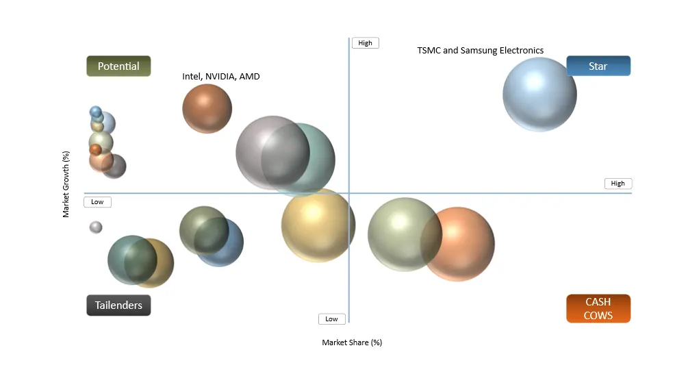
STAR
Stars in the market for nanoscale semiconductors include TSMC and Samsung Electronics because of their combination of advanced node expertise and exposure to the transition to 2nm and below based on GAA technology. Their experience and investments in semiconductor ecosystems as well as exposure to AI and HPC, mobile processing and advanced memory place them well within the high-growth part of the market.
POTENTIAL
Intel, NVIDIA, AMD, SK hynix, Qualcomm, Broadcom, MediaTek and Micron Technology are all classified under Potential players because their success depends increasingly on the use of nanoscale semiconductor technology-based next-generation components such as advanced processors, AI accelerators, mobile processors, HBM and high-density memories. The future positioning in the market will depend on their ability to make use of advanced process nodes, leading-edge fabrication facilities, AI requirements and advanced package integration technology.
Nanoscale Semiconductor Market Dynamics
Driver Impact Analysis
| Driver | Market Growth Impact (%) | Demand Concentration | Impacted Use Case | Strategic Impact |
Rising demand for AI and high-performance computing | 7.80% | Data centers, AI processors, HPC | GPUs, AI accelerators, advanced CPUs | Accelerates investment in advanced process nodes and nanoscale transistor architectures |
Expansion of advanced semiconductor nodes | 6.90% | Leading-edge foundries | 5nm, 3nm, 2nm and below | Drives GAA, nanosheet and next-generation transistor adoption |
Growing semiconductor demand from automotive applications | 5.70% | EVs, ADAS, autonomous vehicles | Automotive processors, sensors, power-management ICs | Increases demand for high-performance and energy-efficient nanoscale chips |
Increasing adoption of edge computing and IoT | 4.80% | Consumer, industrial and connected devices | Edge processors, microcontrollers, sensors | Supports demand for compact, low-power nanoscale semiconductor devices |
Driver: Accelerating Demand for AI and High-Performance Computing Chips
The key factor behind the growth of the nanoscale semiconductor market is the quick growth in applications such as training, inference and high-performance computing which require semiconductors with increased transistor density and significant improvement in performance per watt ratio. Advanced semiconductor solutions like AI GPUs, AI ASICs, NPUs and even CPUs are now employing 3 nm and 2 nm node technology, which is made possible by the use of GAA/Nanoplatelet technology which offers higher transistor density and efficiency. The need for increased computational power in terms of hyperscale data centers, generative AI applications and even autonomous cars is driving up the demand for cutting-edge semiconductor capacity.
Restraint Impact Analysis
| Restraint | Drag on Market Growth (%) | Primary Impact Area | Impacted Use Case | Strategic Impact |
High cost of advanced- node semiconductor manufacturing | 5.90% | Fabrication and capital expenditure | 3nm, 2nm and below | Encourages selective capacity expansion and technology partnerships |
Increasing complexity of nanoscale fabrication | 5.10% | Process development and yield | GAA, nanosheet and advanced transistor manufacturing | Increases R&D requirements and extends technology qualification cycles |
Semiconductor supply-chain and equipment constraints | 4.60% | Equipment and materials availability | Advanced lithography and wafer fabrication | Drives supplier diversification and strategic inventory management |
Low manufacturing yields at leading-edge nodes | 4.20% | Wafer production and profitability | Sub-5nm logic and advanced memory | Encourages process optimization, yield-improvement investments and design-for-manufacturing strategies Bottom of Form |
Restraint: Escalating Cost and Complexity of Advanced-Node Manufacturing
Major restraint in nanoscale semiconductor market is the rapid escalation in the cost of fabrication and intricacy of fabrication process at 3nm, 2nm and sub-2nm nodes. Highly accurate deposition, selective etching, advanced EUV lithography, improved process control, intricate interconnect and power delivery processes, among others, are involved with increased complexity in fabrication process and number of defects that could increase difficulties with yield ramp. High costs of fabs, high costs of advanced equipment, high costs of masks and materials and low initial yields lead to higher costs per functional die and restrict the use of advanced nanoscale technology solutions to valuable applications like AI accelerators, HPC processors and premium mobile chips.
Nanoscale Semiconductor Market Segmentation Analysis
The global nanoscale semiconductor market is segmented based on the Technology, Process Node, Semiconductor Material, Device Type, Wafer Size, Application, End-User and Region.
By Technology
FinFET's Mature Manufacturing Base Sustains Its Dominance Across Advanced Logic Devices
The FinFET Technology is the leading technology in the nanoscale semiconductor market for 2025, with market share of 58%, supported by wide commercial use of FinFET technology in 7nm, 5nm and 3nm generation semiconductors. The mature manufacturing process, proven design flow & EDA/IP infrastructure, high yield performance and wide use of FinFET in CPUs, GPUs, SoC devices, AI accelerators and automotive processors make FinFET technology more established in terms of production base than any other emerging transistor technologies. Despite the rapid growth of GAA technology adoption due to migration to 2nm and below process nodes, FinFET continues to be the leader in 2025.
By Technology
GAA Becomes the Key Architecture for Next-Generation AI and HPC Processors
Gate-All-Around (GAA) is the fastest-growing technology in the electronics industry as semiconductor manufacturers move from FinFET to the nanosheet-based technologies of 2nm and below. GAA technology is expected to grow at a CAGR of 27.5% from 2026 to 2035, as the demand for higher accuracy and better efficiency in AI processes, high-performance computing processes, mobile systems on chips and data center ICs. Commercial use of this technology has already started, as TSMC launched its N2 technology and aims for mass manufacturing by Q4 2025, confirming that GAA will be used the most in the next wave of integrated circuits.
Nanoscale Semiconductor Market Geographical Penetration
Taiwan Nanoscale Semiconductor Market Landscape
Taiwan continues to be the top global center for the production of nanoscale semiconductors with the help of TSMC having all process capabilities for 3nm and 2nm classes of technology, a robust ecosystem of semiconductor equipment and material suppliers and high demand from the side of the consumers of artificial intelligence (AI), high-performance computing (HPC), smartphones and advanced computing technologies. Transition is taking place from FinFET to GAA nanosheets technology in 2nm class while the ecosystem in Taiwan is developing fabrication with the use of EUV lithography, advanced process control, backside power delivery and CoWoS/3D advanced packaging for dense AI processors.
U.S. Nanoscale Semiconductor Market Landscape
The United States nanoscale semiconductor market is solidifying its position in next-generation semiconductor manufacturing with the help of Intel 18A RibbonFET technology and TSMC's growing Arizona manufacturing facilities. In addition to that, the U.S. nanoscale semiconductor market features a rich ecosystem of AI chip makers, semiconductor equipment manufacturers, EDA providers and advanced packaging firms. Specifically, the market is heavily oriented towards 2nm class and below scaling, GAA/RibbonFET architectures, EUV-based manufacturing, backside power delivery and advanced 2.5D/3D packaging for AI accelerators and HPC processors. In parallel, semiconductor-related government policies are supporting advanced node manufacturing within the country. The existence of firms like Intel, NVIDIA, AMD, Qualcomm, Applied Materials, Lam Research and KLA provides strength to the U.S. in both the design of nanoscale chips and the essential supply chain of manufacturing technology.
South Korea Nanoscale Semiconductor Market Outlook
South Korea plays an important role as the nanoscale semiconductor center due to Samsung’s advanced foundry technology and SK hynix’s advanced memory technology, specifically HBM. The development of the 2nm GAA manufacturing process technology, extreme UV lithography-based manufacturing, DRAM/HBM scaling and advanced packaging is currently being developed in Korea along with Samsung’s roadmap for further advancement beyond 2nm. The growing need for AI accelerators, HPC processors, smartphones and HBM is leading to the development of denser semiconductors, whereas the Korean ecosystem comprising foundries, memory makers, material providers and equipment makers positions Korea well during the transition to sub-2nm logic and next-generation memory technologies.
Japan Nanoscale Semiconductor Market Outlook
The Japanese efforts to re-establish themselves in leading-edge nanometer semiconductor manufacturing have been bolstered by the 2nm GAA project of Rapidus and the well-developed ecosystem in Japan comprising of semiconductor materials, equipment, photomasks and precision manufacturing technologies. The 2nm GAA project of Rapidus encompasses the development of 2nm GAA process, EUV-enabled fabrication, integration of chiplets and 2.5D/3D packaging, thus providing a roadmap to develop next-generation logic devices domestically. The strengths of Japan in silicon wafers, photoresists, semiconductor chemicals, manufacturing equipment and precision parts provide vital assistance in nanometer manufacturing, whereas technology programs supported by the government have enabled the development of a 2nm ecosystem domestically.
China Nanoscale Semiconductor Market Trends
Chinese nanoscale semiconductor industry is becoming influenced more by Chinese domestic advanced node development, semiconductors equipment localization and increased demand for AI and high-performance computing chips. SMIC is still China’s leading advanced node foundry with 7nm class manufacturing technology, but Hua Hong is also developing 7nm class production. In terms of equipment, Chinese companies have started mass production of their domestic immersion DUV lithography system as part of the attempt to localize manufacturing technologies due to the limitations on exports. The market is thus changing due to advanced node process technology development, domestic lithography and manufacturing equipment development, AI chip manufacturing and localized manufacturing ecosystem. The limitation on leading edge lithography is still an issue which influences China’s progress towards 2nm class manufacturing.
Nanoscale Semiconductor Market Competitive Landscape
- TSMC leads in the race for advanced nodes by having the 3nm node contributing 24% to the company’s wafer revenues in 2025 while 2nm N2 moving into high volume production by Q4 2025, further cementing its leadership in GAA nanoscale production.
- Samsung Electronics relies on an integrated GAA and advanced memory approach, wherein the company's 2nm GAA logic process technology combines with its advanced DRAM and HBM solutions for AI and high-performance computing applications.
- Intel differentiates itself using RibbonFET and PowerVia technology, as Intel 18A process incorporates both the GAA transistor design and the PowerVia technology to cater to the requirements of performance and efficiency.
- Requirements for next-generation technology nodes such as 3nm and 2nm technology along with advanced packaging and high bandwidth memory are fueled by companies like NVIDIA, AMD, Qualcomm and Broadcom using artificial intelligence accelerators, HPC processors, mobile SoCs and ASICs.
- The competition among these firms is moving from just transistor scaling to compete over other factors such as full stack nanotechnology integration including GAA technology, back-side power delivery, EUV technology capability, yields, advanced packaging, chiplet design and performance-per-watt.
Public Company Q1-Q2 2026 Performance Comparison
In the table presented below, five public companies that are affected either directly or strategically by the nanoscale semiconductor market have been compared. The financial performance is based on company-wide or semiconductor division data, since the companies do not break down their revenue generated specifically from nanoscale semiconductors. The comparison therefore separates the financial performance from the involvement in 2nm/3nm fabrication, GAAFET technology, advanced node logic and AI/HPC chips.
| Company | Q1–Q2 2026 Performance | Nanoscale Semiconductor-Relevant Exposure | Key Performance Driver |
| TSMC | Revenue: US$40.20 billion, up 33.7% YoY; net income: approximately US$16.7 billion, up 77.4% YoY. | 2nm and 3nm leading-edge foundry manufacturing, GAA nanosheet technology and advanced packaging | AI/HPC demand, advanced-node migration and increasing 2nm production |
| Samsung Electronics | Revenue: approximately US$119.5 billion; operating profit: approximately US$62.4 billion. | 2nm GAA, advanced-node foundry, logic semiconductors, advanced DRAM and HBM | AI-driven semiconductor demand, higher memory prices and advanced-node foundry opportunities |
| Intel | Revenue: US$16.1 billion, up 25% YoY; non-GAAP EPS: US$0.42. | 18A RibbonFET GAA, PowerVia backside power delivery, advanced logic and Intel Foundry | 18A production ramp, advanced-process investment, AI/server demand and foundry expansion |
| AMD | Revenue: US$11.5 billion, up 50% YoY; Data Center revenue: US$6.7 billion, up 107% YoY. | Leading-edge CPUs, GPUs, AI accelerators, chiplets, advanced packaging and future 2nm platforms | AI infrastructure expansion, EPYC server demand and Instinct accelerator adoption |
| SK hynix | Revenue: approximately US$53.0 billion, up 257% YoY; operating profit: approximately US$40.5 billion. | HBM4/HBM3E, advanced DRAM, high-density memory stacking and AI accelerator memory | AI-server demand, HBM adoption, higher-value memory products and advanced stacking |
Note: Financial periods differ because the companies use different fiscal calendars. The comparison uses the latest Q1–Q2 2026 results available and should not be interpreted as standalone nanoscale-semiconductor revenue. TSMC and Samsung have the most direct exposure to leading-edge node manufacturing, while Intel has direct advanced-process exposure and AMD/SK hynix benefit strongly from demand for leading-edge compute and memory technologies.
Key Companies of Nanoscale Semiconductor Market
- Taiwan Semiconductor Manufacturing Company (TSMC) (Taiwan)
- Intel Corporation (United States)
- Samsung Electronics (South Korea)
- NVIDIA Corporation (United States)
- Qualcomm (United States)
- Advanced Micro Devices (AMD) (United States)
- Broadcom (United States)
- Micron Technology (United States)
- SK hynix (South Korea)
- GlobalFoundries (United States)
- United Microelectronics Corporation (UMC) (Taiwan)
- SMIC (China)
- MediaTek (Taiwan)
- Apple (United States)
- Marvell Technology (United States)
- Texas Instruments (United States)
- Renesas Electronics (Japan)
- STMicroelectronics (Switzerland)
- NXP Semiconductors (Netherlands)
- Infineon Technologies (Germany)
Company Profiles
TSMC
TSMC is a major player in the pure-play semiconductor foundry business and a key player in the manufacture of semiconductors at the nanoscale level with advanced node manufacturing that includes 3nm and 2nm. The N2 process by TSMC uses a Gate-All-Around nanosheet design and went into mass production in Q4 2025, while TSMC develops the N2P and A16 processes.
Competitive priorities include accelerating yield improvement for 2nm processes, building advanced node capacity, adding advanced packaging capability like CoWoS, performance-per-watt and keeping ahead technologically in GAA process scaling.
Samsung Electronics
Samsung is one of the leading integrated semiconductor manufacturers that compete in advanced node logic, foundry, DRAM and HBM segments. The 2 nm GAA process of Samsung is aimed at high-performance computing, mobile processors and AI. The integration of logic manufacturing and advanced memory of Samsung creates an ideal platform for next-generation AI systems.
Competitive priorities are increasing yield of 2nm GAA technology, attracting advanced node foundry customers, expanding HBM technology capacity, combining logic and memory technologies and positioning itself in AI and HPC market segments.
Intel
Nanoscale semiconductor technology leadership efforts by Intel involve their 18A process that features RibbonFET GAA transistor architecture with PowerVia backside power delivery scheme. Not only does Intel utilize its process technology for its own CPU and AI products, but also as the backbone technology for developing its Intel Foundry services for external customers.
The competitive priorities for Intel include ramping 18A production, improving process yield, finding external foundry customers, enhancing backside power delivery and development of future nodes after 18A.
NVIDIA
NVIDIA represents a key demand driver for nanometer semiconductors through its AI GPUs, accelerated computing platforms and data center processors. Its evolving architecture needs state-of-the-art nodes, advanced packaging, HBM and high interconnect density. Thus, semiconductor process scaling becomes an important factor in meeting performance and power efficiency objectives.
Priority areas include ensuring availability of leading-edge foundry capacity, achieving higher transistor and compute densities, implementing HBM and advanced packaging, enhancing performance per watt and developing next-generation AI accelerators.
AMD
AMD is a well-known fabless semiconductor company that utilizes latest manufacturing technologies for its EPYC CPUs, Instinct AI accelerators, Ryzen processors and chiplet architectures. The reliance on cutting-edge foundry processes necessitates nanometer-scale transistor scaling, advanced packaging and chiplet integration for enhancing computing performance with control of power consumption.
Priority areas are adoption of next generation process nodes, improvements in AI accelerator performance, chiplet architecture optimization, increase in compute density and performance per watt.
SK Hynix
SK hynix is a leading producer of advanced memory technology and its HBM3E and HBM4 technologies have become very important for AI accelerators with state-of-the-art logic. The company’s nanotechnology semiconductor exposure is limited to advanced DRAM technology development, high memory density stacking and advanced HBM technology that allows higher bandwidth and memory capacity for AI and HPC technologies.
Competitive focus includes scaling up HBM4 production, increasing memory stack density, increasing yields and bandwidths, advancing hybrid bonding technologies and aligning high memory density production with the booming demand of AI accelerators..
Nanoscale Semiconductor Market Major Pain Points
- Sub-2nm yield and process-variability challenges: GAA nanosheets, tighter dimensioning, EUV stochastic defects and novel materials present increasingly difficult problems regarding defect management and yield consistency below 2nm.
- Escalating cost per good die: The economics of advanced nodes are starting to become less attractive as the wafer, mask and lithography costs grow more rapidly than improvements in node performance.
- Extreme dependence on advanced lithography: EUV and future High-NA EUV systems demand highly expensive tools and create a number of throughput, stochastic defect, overlay and process integration challenges.
- Interconnect and power-delivery bottlenecks: Smaller transistors do not necessarily result in improved chip performance since the resistance of wire and movement of signals, power delivery and heat become a bigger issue for nanoscale chips.
- Increasing design-to-manufacturing complexity: GAA and CFET technologies demand closer integration between the design of transistors, PDKs, EDA, process rules, metrology and advanced packaging, which increases the time it takes to develop new designs and limits the number of organizations that can afford to adopt the cutting edge technology.
Nanoscale Semiconductor Market Recent Developments
- August 2026-SK hynix: SK hynix announced the initiation of mass production for 12-stack HBM4 and the customer qualification of 16-stack HBM4. This is indicative of the fast development in memory stacking technology.
- July 2026-Samsung Electronics: Samsung made strides in its 2nm GAA foundry roadmap aimed at high-performance computing and AI, thus intensifying competition in the most advanced foundry business.
- July 2026-AMD: AMD unveiled its Zen 6 processor family for the EPYC Venice platform, which marked a significant step towards the TSMC 2nm node process technology in future server CPUs and HPC.
- January 2026-Intel: Intel shifted to 18A process node with RibbonFET GAA transistors and PowerVia backside power distribution for high-volume manufacturing, with Panther Lake being a noteworthy commercial product based on this platform.
- December 2025-TSMC: TSMC began production of 2nm (N2) using GAA nanosheets, signaling a significant move from FinFET to the 2nm logic nanosheets technology on the commercial front.
Analyst View / Opinion on Nanoscale Semiconductor Market
- 2nm GAA is becoming the core commercial scaling platform: The industry is transitioning decisively from FinFETs to GAA nanosheet technology, which is making process development in 2nm-class nodes in which yield and power performance will be the major competitive indicators for advanced digital technologies.
- Process-node leadership alone will no longer determine competitiveness: In the sub-2nm regime, competitiveness will increasingly depend on the overall performance of transistors, interconnects, power delivery, packaging and memories.
- Advanced packaging is becoming inseparable from nanoscale scaling: CoWoS, chiplets, hybrid bonding and 3D integration are getting ever more important because simple further shrinking of transistors cannot solve the problems related to AI computing, bandwidth and power delivery.
- CFET represents the next major architectural inflection point: Forksheet and CFET architectures are getting more popular as possible replacements for GAA architecture, with CFETs allowing vertical stacking of nFET and pFET devices.
- Yield will become a key competitive differentiator: In view of the complexity and cost involved in the production at 2nm and sub-2nm level, commercial yields would be a critical factor in determining the competitiveness of nanoscale semiconductor manufacturers.
Nanoscale Semiconductor Market Target Audience
| INDUSTRY | WHO SHOULD BUY THIS REPORT? | REASON TO BUY THIS REPORT |
| Semiconductor Manufacturing | Semiconductor Foundries | Assess advanced-node capacity, technology adoption and competitive positioning |
Integrated Device Manufacturing | IDMs | Evaluate nanoscale process development, investment priorities and technology roadmaps |
| Fabless Semiconductors | Fabless Chip Companies | Identify suitable foundry partners and emerging nanoscale semiconductor technologies |
| Semiconductor Equipment | Semiconductor Equipment Manufacturers | Quantify demand for EUV, deposition, etching, metrology and other advanced fabrication equipment |
| Semiconductor Materials | Semiconductor Material Suppliers | Identify opportunities for advanced materials such as SiGe, 2D materials and compound semiconductors |
AI & High-Performance Computing | AI Chip Developers and HPC Companies | Evaluate demand for advanced processors, AI accelerators and high-density nanoscale chips |
| Memory Semiconductors | DRAM and NAND Manufacturers | Assess nanoscale scaling opportunities and emerging memory technologies |
| Consumer Electronics | Smartphone, Laptop and Wearable Manufacturers | Understand availability and adoption of smaller, faster and more power-efficient semiconductor devices |
| Automotive Electronics | Automotive OEMs and Tier-1 Suppliers | Evaluate nanoscale semiconductor demand for ADAS, autonomous driving and EV electronics |
| Telecommunications | Telecom Equipment Manufacturers | Assess demand for advanced RF, communication and high-performance semiconductor technologies |
Why Choose DATAM?
- Data-Driven insights: Dive into detailed analyses with granular insights such as pricing, market shares and value chain evaluations, enriched by interviews with industry leaders and disruptors.
- Post-Purchase Support and Expert Analyst Consultations: As a valued client, gain direct access to our expert analysts for personalized advice and strategic guidance, tailored to your specific needs and challenges.
- White Papers and Case Studies: Benefit quarterly from our in-depth studies related to your purchased titles, tailored to refine your operational and marketing strategies for maximum impact.
- Annual Updates on Purchased Reports: As an existing customer, enjoy the privilege of annual updates to your reports, ensuring you stay abreast of the latest market insights and technological advancements. Terms and conditions apply.
- Specialized Focus on Emerging Markets: DataM differentiates itself by delivering in-depth, specialized insights specifically for emerging markets, rather than offering generalized geographic overviews. The approach equips our clients with a nuanced understanding and actionable intelligence that are essential for navigating and succeeding in high-growth regions.
- Value of DataM Reports: Our reports offer specialized insights tailored to the latest trends and specific business inquiries. The personalized approach provides a deeper, strategic perspective, ensuring you receive the precise information necessary to make informed decisions. The insights complement and go beyond what is typically available in generic databases.
What DATAM Uniquely Provides
- 2nm-to-sub-2nm technology benchmarking: Comparison of GAA Nanosheet, Forksheet and CFET technologies based on their technological maturity and commercial readiness.
- Advanced-node cost and yield intelligence: Analysis of wafer costs, yield sensitivity, process complexity and its impact on cost per good die.
- Nanoscale manufacturing value-chain mapping: Relates EUV/High NA EUV, ALD, selective etch, metrology, materials, backside power and advanced packaging to certain process needs.
- AI-to-nanoscale demand mapping: Measures impact of AI accelerators, custom ASICs and HPC processors on 2nm/3nm capacities, advanced packaging and technologies.
- Beyond-FinFET opportunity assessment: Separates scalable GAA technologies from future forksheet, CFET, 2D materials and hybrid integration technologies, enabling organizations to identify their short-, mid- and long-term opportunities.