


Paras Semiconductors Private Limited, a subsidiary of Paras Defence and Space Technologies Ltd., has announced plans to establish a greenfield advanced semiconductor packaging facility in Madhya Pradesh with a proposed investment of approximately ₹6,200 crore.
The proposed Outsourced Semiconductor Assembly and Test (OSAT) facility will be developed in the Indore-Ujjain region of Madhya Pradesh and aims to enhance India's semiconductor manufacturing capabilities by supporting advanced integrated circuit (IC) packaging, assembly, and testing operations.
The project follows a Memorandum of Understanding (MoU) between Paras Semiconductors and the Madhya Pradesh State Electronics Development Corporation (MPSeDC), operating under the state's Department of Science and Technology, to facilitate the development of the advanced semiconductor facility.
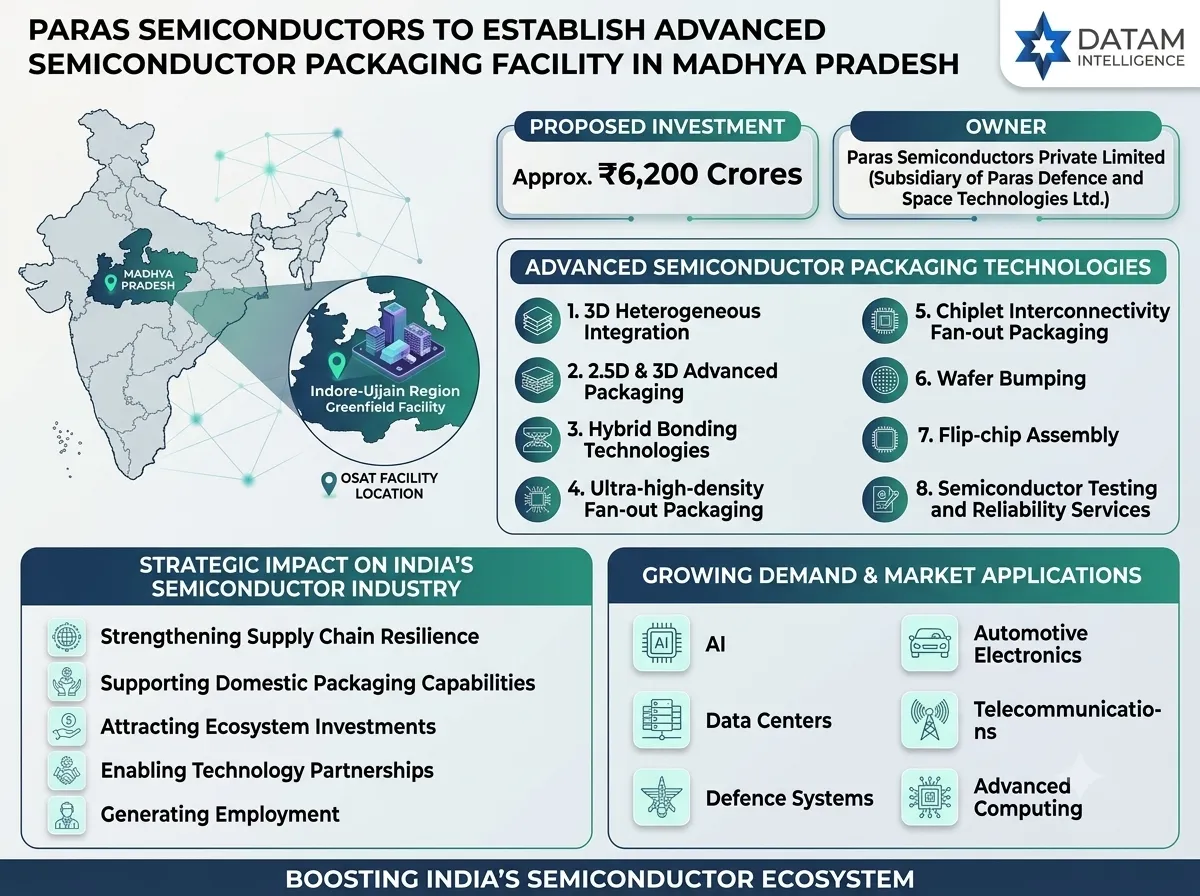
Advanced Semiconductor Packaging Technologies to Drive Next-Generation Chip Manufacturing
The upcoming OSAT facility is expected to focus on several advanced semiconductor technologies, including:
- 3D heterogeneous integration
- 2.5D and 3D advanced packaging
- Hybrid bonding technologies
- Ultra-high-density fan-out packaging
- Chiplet integration
- Wafer bumping
- Flip-chip assembly
- Semiconductor testing and reliability services
These technologies are becoming increasingly important as industries demand higher-performance chips for artificial intelligence (AI), automotive electronics, data centers, telecommunications, defence systems, and advanced computing applications.
Madhya Pradesh Emerges as an Emerging Semiconductor Manufacturing Hub
The investment represents a significant step toward expanding India's semiconductor value chain beyond traditional electronics manufacturing centers. The Madhya Pradesh government has supported the project through collaboration with MPSeDC, including land allocation initiatives for the proposed facility.
The development aligns with India's broader semiconductor strategy focused on building domestic capabilities across chip design, manufacturing, advanced packaging, and testing infrastructure.
With increasing global demand for semiconductor chips driven by artificial intelligence, cloud computing, electric vehicles, and consumer electronics, advanced packaging facilities such as OSAT plants are becoming critical components of the global semiconductor supply chain.
Strategic Impact on India’s Semiconductor Industry
The Paras Semiconductors OSAT facility is expected to create opportunities across multiple areas, including:
- Strengthening India's semiconductor supply chain resilience
- Supporting domestic chip packaging and testing capabilities
- Attracting semiconductor ecosystem investments
- Enabling technology partnerships and innovation
- Supporting high-skilled employment generation
Advanced packaging is gaining importance globally as semiconductor companies increasingly adopt chiplet architectures and heterogeneous integration approaches to overcome traditional scaling limitations.
Growing Demand for OSAT and Advanced Semiconductor Packaging Market
The global semiconductor market industry is witnessing rapid transformation as demand rises for high-performance computing, AI processors, automotive chips, and connected devices. OSAT providers play a crucial role by offering specialized assembly, packaging, and testing capabilities required for modern semiconductor applications.
India's growing focus on semiconductor infrastructure development is expected to accelerate opportunities for semiconductor equipment manufacturers, packaging technology providers, electronics manufacturers, and investors seeking exposure to the expanding chip ecosystem.
Analyst View: India’s Semiconductor Supply Chain Moves Toward Advanced Packaging
The proposed Paras Semiconductors facility highlights a strategic shift toward developing advanced semiconductor back-end capabilities in India. As semiconductor demand continues to expand across AI infrastructure, automotive electronics, defence technologies, and digital transformation initiatives, investments in OSAT and advanced packaging infrastructure are expected to become increasingly important.
Frequently Asked Questions
What is the Paras Semiconductors OSAT facility in Madhya Pradesh?
Paras Semiconductors is planning a ₹6,200 crore advanced OSAT facility in the Indore-Ujjain region of Madhya Pradesh to provide semiconductor packaging, assembly, and testing services using next-generation technologies.
What technologies will the Paras Semiconductors facility support?
The facility will support advanced semiconductor packaging technologies including 3D heterogeneous integration, chiplet integration, hybrid bonding, fan-out packaging, wafer bumping, flip-chip assembly, and testing services.
Why is OSAT important for India’s semiconductor industry?
OSAT facilities help strengthen semiconductor supply chains by enabling advanced chip packaging and testing, which are essential stages in semiconductor production.