


A few years ago, the hardest question was whether chip designers could obtain enough leading-edge wafer capacity. Today, producing the transistor is only part of the problem. AI accelerators need logic dies, high-bandwidth memory, substrates, interposers, thermal interfaces, and increasingly sophisticated interconnects to operate as one high-performance system.
That makes advanced semiconductor packaging one of the most important constraints between an AI chip design and a deployable AI server.
DataM Intelligence estimates that the global advanced packaging semiconductor market reached US$22.48 billion in 2025 and could reach US$46.98 billion by 2035, expanding at a CAGR of 7.8% during 2026-2035.
However, the interesting opportunity is not simply participating in a larger packaging market.
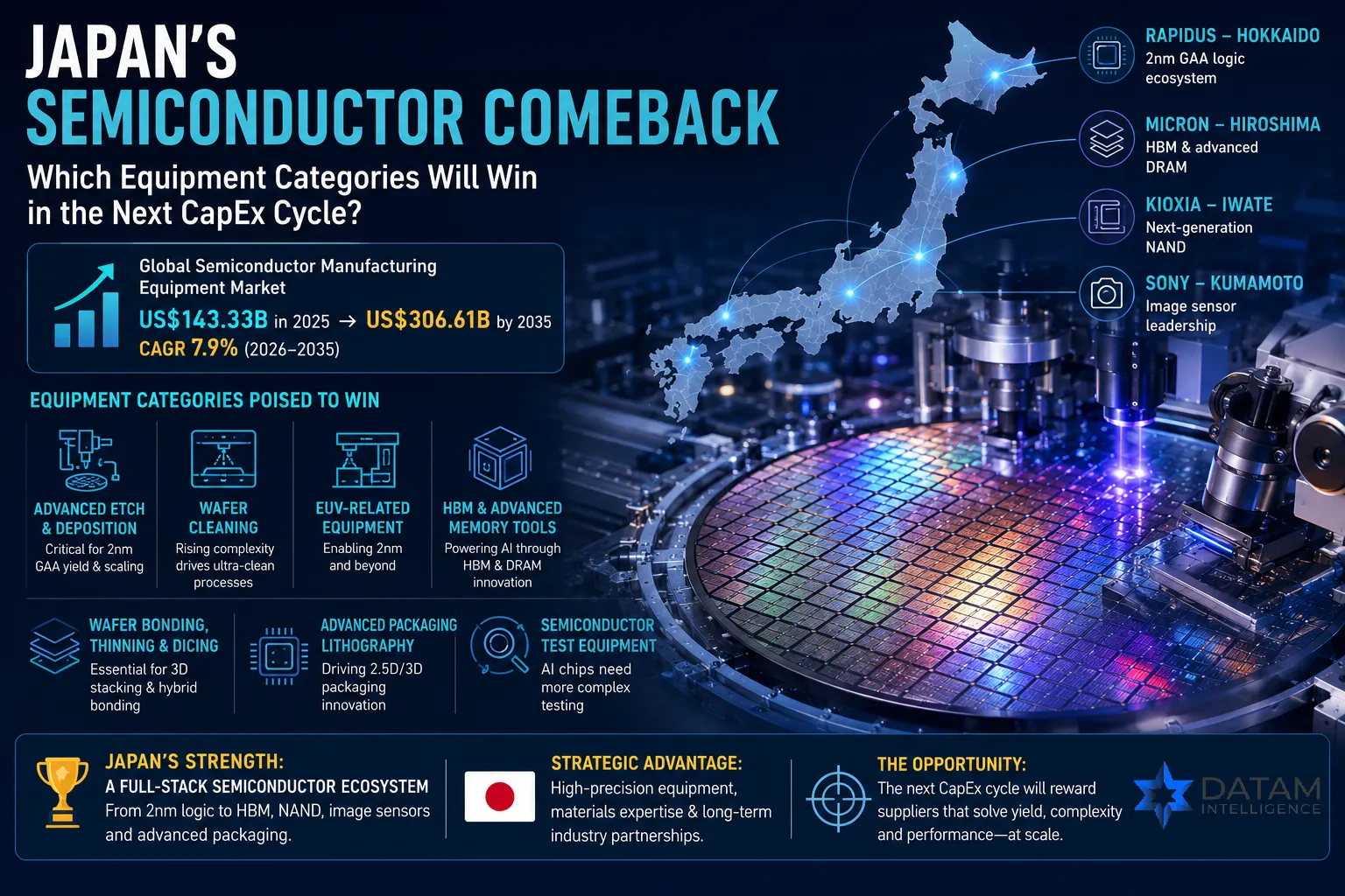
Japan already controls or influences critical parts of the packaging stack: advanced substrates, insulating materials, photoresists and chemicals, precision wafer processing, cleaning, bonding, testing, and manufacturing equipment.
The strategic question is therefore changing from "Will advanced packaging demand increase?" to something much more useful:
Where is the next packaging bottleneck forming, and which Japanese companies are positioned to remove it?
Request Exclusive Sample on Advanced Packaging Semiconductor Market
Japan's 2026 Packaging Story Starts With Rapidus-but It Does Not End There
Rapidus has become the clearest signal that Japan no longer intends to separate leading-edge wafer fabrication from advanced packaging.
On April 11, 2026, Rapidus formally opened both its Analysis Center and Rapidus Chiplet Solutions in Chitose, Hokkaido. Rapidus Chiplet Solutions is not simply a laboratory attached to its 2nm fab. It is intended as an advanced back-end R&D hub supporting chiplet packaging and mass-production process development.
One detail deserves far more attention than it has received.
Rapidus has already produced a prototype 600 mm-square organic insulating-film RDL interposer panel and is moving into full-scale verification of 2.xD and 3D package manufacturing processes, alongside package-design and test technologies.
That matters because the industry's packaging economics may eventually move beyond processing only circular wafers.
Larger rectangular panels could allow more interposers to be processed simultaneously and potentially improve manufacturing economics for large AI packages. But scaling panel-level packaging also introduces difficult problems involving warpage, pattern accuracy, materials uniformity, handling and yield.
In other words, Japan is not only trying to increase packaging capacity.
It is experimenting with how advanced packaging itself could be manufactured differently.
Japan's Ministry of Economy, Trade and Industry reinforced the direction in April 2026 by approving an increased budget following its stage-gate review of Rapidus's 2nm program, including the project specifically dedicated to 2nm-generation chiplet package design and manufacturing technology.
The government has effectively acknowledged that a domestic 2nm capability without an advanced packaging capability would leave a critical part of the value chain outside the country.
The Real Bottleneck May Be the Package Substrate
The AI semiconductor discussion tends to focus on HBM supply and foundry capacity.
Substrates receive considerably less attention.
That could be a mistake.
In February 2026, IBIDEN approved an investment plan of roughly ¥500 billion between fiscal 2026 and fiscal 2028 to expand high-performance IC package substrate capacity, particularly for AI and high-performance servers.
The first phase includes around ¥220 billion of investment, primarily at the Gama Plant and other sites, with capacity expected to begin coming online sequentially from fiscal 2027.
That is not a small incremental production upgrade.
It demonstrates how much larger and technically demanding AI package substrates are becoming.
An advanced AI accelerator package has to connect increasingly complex processors and memory systems while controlling electrical loss, mechanical stress, and heat. As package size increases, substrate layer counts, wiring density, and reliability requirements become harder to manage.
This means additional CoWoS-class or chiplet packaging capacity cannot simply be created by buying another bonding machine.
The substrate, interposer, materials, bonding, and test capacity must expand together.
That is the point where many semiconductor capacity forecasts become misleading.
The bottleneck is not necessarily the process with the lowest installed capacity.
It is the process with the lowest qualified, high-yield capacity.
TSMC Is Using Japan as an Advanced Packaging R&D Bridge
Japan's packaging advantage is visible in another unusual decision.
TSMC established its Japan 3DIC R&D Center in Tsukuba, Ibaraki, as its first R&D facility outside Taiwan equipped with a cleanroom.
The center works with Japanese companies, research organizations, and universities on next-generation 3D silicon stacking and advanced packaging. Its research areas include substrate development, thermal interface materials, mold compounds, underfill, solder, process equipment, metrology, and inspection.
Importantly, TSMC explicitly connects the center's work with technologies such as CoWoS and TSMC 3DFabric, including the integration of HBM with advanced logic devices.
This says something important about Japan's competitive position.
Japan does not have to displace Taiwan's packaging ecosystem to benefit from advanced packaging.
It can become the place where the next generation of materials, substrates, and equipment used by that ecosystem gets developed and qualified.
That is potentially a much stronger commercial position than trying to replicate every OSAT manufacturing line domestically.
Resonac Is Trying to Change How Packaging Technology Gets Qualified
One of the most interesting Japanese advanced packaging strategies is coming from Resonac.
Rather than developing every technology internally, Resonac is building shared development environments where materials companies, equipment manufacturers and customers can test entire packaging flows together.
Its JOINT3 consortium had expanded to 28 participating companies by May 2026 and is focused on developing materials, equipment and design tools for panel-level organic interposers.
The associated APLIC development hub in Ibaraki is designed around a prototype line for approximately 515 × 510 mm panel-level organic interposers.
But Resonac's more disruptive commercial experiment may be happening outside Japan.
In April 2026, it opened an advanced packaging R&D center in Silicon Valley through the US-JOINT consortium, bringing Japanese materials and equipment companies physically closer to fabless semiconductor companies and potential customers.
Resonac says one goal is to reduce proof-of-concept cycles that could previously take six months to around one month.
This is a major change in semiconductor materials selling.
The old model was: develop a material, send samples, wait for evaluation, and gradually pursue qualification.
The emerging model is: bring the customer, materials suppliers, and equipment companies into one packaging line and qualify the system together.
For Japanese suppliers, shortening qualification time could become almost as important as improving material performance.
Request for Customized Sample According to your Business Needs: https://www.datamintelligence.com/customize/advanced-packaging-semiconductor-market
Hybrid Bonding Is Moving From R&D Topic to Equipment Business
As chiplets become more tightly integrated, conventional solder-based interconnects eventually face limits in pitch, bandwidth and energy efficiency.
That is why copper hybrid bonding is receiving so much attention.
Tokyo Electron already offers 300 mm bonding systems supporting both fusion bonding and Cu hybrid bonding. It is also expanding tools around temporary bonding, debonding, edge trimming and package testing.
The company's financial expectations show how significant the transition could become.
At its 2026 shareholders' meeting, Tokyo Electron said its wafer-bonding-related business had tripled during the previous two years, generated roughly ¥30 billion in sales in the preceding fiscal year and was expected to rise another 60% during the current fiscal year. TEL is targeting advanced packaging-related equipment sales of more than ¥300 billion by 2030.
SCREEN is pursuing the same technological shift from another direction.
After acquiring Nikon's wafer-bonding R&D business, SCREEN has been combining high-precision bonding capability with its own low-temperature processing, direct imaging, cleaning and surface-preparation technologies.
This competition matters because hybrid bonding is not simply about placing two wafers together.
Surface cleanliness, wafer warpage, alignment accuracy, copper interface quality and bonding temperature all affect yield.
Japan's advantage could therefore come from combining bonding equipment with the cleaning, surface treatment and precision-control technologies surrounding it.
Advanced Packaging Is Also Creating a New Test Economics
There is another bottleneck forming after the wafer has been processed: deciding which dies are good enough to package.
Putting a defective die into an expensive multi-chip package can destroy the value of several other perfectly functional dies and HBM stacks.
That makes Known Good Die testing economically more important as package value rises.
Tokyo Electron launched its Prexa SDP singulated device prober in April 2026 specifically to test individual unpackaged devices for 2.5D and 3D packaging. The system includes thermal-control technology designed for high-heat-generating devices.
This is a good example of how AI changes the equipment value chain.
Test is no longer simply the final quality-control stage.
It becomes a way of preventing expensive packaging capacity and HBM from being wasted on a defective chiplet.
That gives Japan's equipment companies an opportunity to monetize the rising cost of failure inside advanced packages.
DISCO Shows Why Precision Processing Matters More as Chips Become Thinner
High-performance packaging also requires dies to become thinner.
That makes grinding, dicing and laser processing strategically important.
DISCO announced in March 2026 that cumulative shipments of its laser saws had exceeded 4,000 systems. More importantly, the pace of shipments for the latest 2,000 systems was nearly three times faster than for the first 2,000.
The company linked rising adoption to advanced logic and high-density memory applications requiring low-damage, high-precision processing, including ultra-thinned memory devices.
HBM illustrates why.
Stacking more memory dies while keeping the total package height manageable requires extremely thin silicon. Once wafers become thinner, mechanical handling and cutting become more difficult.
A process that once looked like conventional wafer preparation therefore becomes a critical part of advanced package yield.
ABF Gives Japan an Unusual Materials Advantage
Not every advanced packaging leader looks like a semiconductor company.
Ajinomoto is one of the best examples.
Its Ajinomoto Build-up Film, or ABF, is an interlayer insulation material used in high-performance semiconductor package substrates. Ajinomoto says its material holds a share approaching 100% in its addressable interlayer insulation market for many computing applications.
This becomes strategically more important as AI accelerators require larger and more complex substrates.
Future ABF generations need to support finer wiring, lower electrical losses, thermal stability and increasingly complicated substrate structures.
The lesson is important for understanding Japan's packaging position:
Japan's leverage does not come from one national champion.
It comes from multiple narrowly specialized technologies that become extremely difficult to replace once qualified into a semiconductor manufacturing process.
Top Companies in Advanced Packaging in Japan
For companies, investors and semiconductor buyers tracking the top companies in advanced packaging in Japan, the most important names span several different parts of the value chain rather than one single OSAT category.
Rapidus - building domestic 2nm chiplet, RDL interposer and 2.xD/3D package-development capabilities in Hokkaido.
IBIDEN - expanding high-performance package-substrate capacity for AI and high-performance servers through a major FY2026-FY2028 investment cycle.
Shinko Electric Industries - developing high-density organic packages, glass-core substrates, optical chiplets and co-packaged optics; its 2026 technology showcase included i-THOP, glass-core substrates and optical-chiplet technologies.
Resonac Holdings - creating shared advanced-packaging development platforms around organic interposers, materials and faster customer qualification.
Ajinomoto / Ajinomoto Fine-Techno - a strategically important supplier of ABF insulation materials used in high-performance semiconductor package substrates.
Tokyo Electron - expanding across wafer bonding, hybrid bonding, debonding, edge processing and Known Good Die testing for 2.5D and 3D integration.
SCREEN Holdings - building an advanced packaging portfolio around direct imaging, cleaning, surface preparation, and increasingly wafer bonding. Its DW-3100 supports both wafer and square-panel formats with sub-1 µm imaging precision.
DISCO - positioned around grinding, dicing and laser processing as HBM and other advanced packages require increasingly thin and precisely processed dies.
NAMICS, Toray Industries and other Japanese specialty-material suppliers also remain important participants as underfill, adhesives, thermal materials and low-loss package materials become more demanding.
Together, these companies show why Japan's opportunity is broader than semiconductor assembly.
Where Should Japan Add Advanced Packaging Capacity First?
The answer is not simply "more packaging lines."
Japan needs to increase capacity at the processes where qualification and yield are most likely to restrict AI chip output.
That currently points toward five areas.
First, high-end IC package substrates need additional qualified capacity as AI packages become larger.
Second, RDL and interposer manufacturing will require new approaches, including panel-level processing.
Third, hybrid bonding and wafer/chip bonding need to move from development lines into high-yield production.
Fourth, thermal management and advanced materials must evolve with package power density.
And fifth, Known Good Die and package-level testing need to scale before increasingly expensive chiplets and HBM stacks are assembled.
The mistake would be to treat each bottleneck independently.
An extra bonding line has little value if substrates are unavailable. More substrates do not solve the problem if thermal limits prevent the package from operating. Additional HBM capacity can still be wasted if Known Good Die testing cannot prevent defective chiplets from entering the package.
The real requirement is synchronized packaging capacity.
Japan's Biggest Advanced Packaging Advantage May Be Qualification Speed
Taiwan remains enormously powerful in foundry-integrated advanced packaging. South Korea has deep memory integration capabilities. The United States is investing heavily in domestic packaging R&D and manufacturing.
Japan needs a different competitive strategy.
Its strongest position may be to become the world's fastest place to develop, test, and qualify the materials and equipment required for next-generation packages.
Rapidus Chiplet Solutions, TSMC's Tsukuba 3DIC center, AIST's hybrid-packaging infrastructure, Resonac's JOINT platforms and equipment initiatives from Tokyo Electron and SCREEN are beginning to create that environment. AIST's latest hybrid packaging hub includes capabilities for heterogeneous bonding, silicon interposers, glass and resin interposers, and other advanced integration technologies.
That changes the commercial opportunity.
The future winner may not be the company with the largest packaging factory.
It could be the supplier that gets its substrate, bonding technology, insulating film, thermal material, test process or manufacturing tool qualified first into the next AI accelerator architecture.
Once qualification occurs, replacing that technology can be difficult, expensive, and risky.
That is where Japan's real packaging leverage lies.
The advanced packaging semiconductor market may reach US$46.98 billion by 2035, but Japan's opportunity will not be determined by market size alone.
It will be determined by which companies solve the industry's hardest package-level problems before those problems become production bottlenecks.
And right now, the battle is moving rapidly toward substrates, RDL, panel-level processing, hybrid bonding, ultra-thin die preparation, thermal management, and Known Good Die testing.
For Japan, advanced packaging is no longer the back end of semiconductor manufacturing.
It is becoming one of the front lines of the AI semiconductor race.
Read the Complete Research Report: https://www.datamintelligence.com/research-report/advanced-packaging-semiconductor-market