Through-Silicon Via (TSV) Technology Market Overview
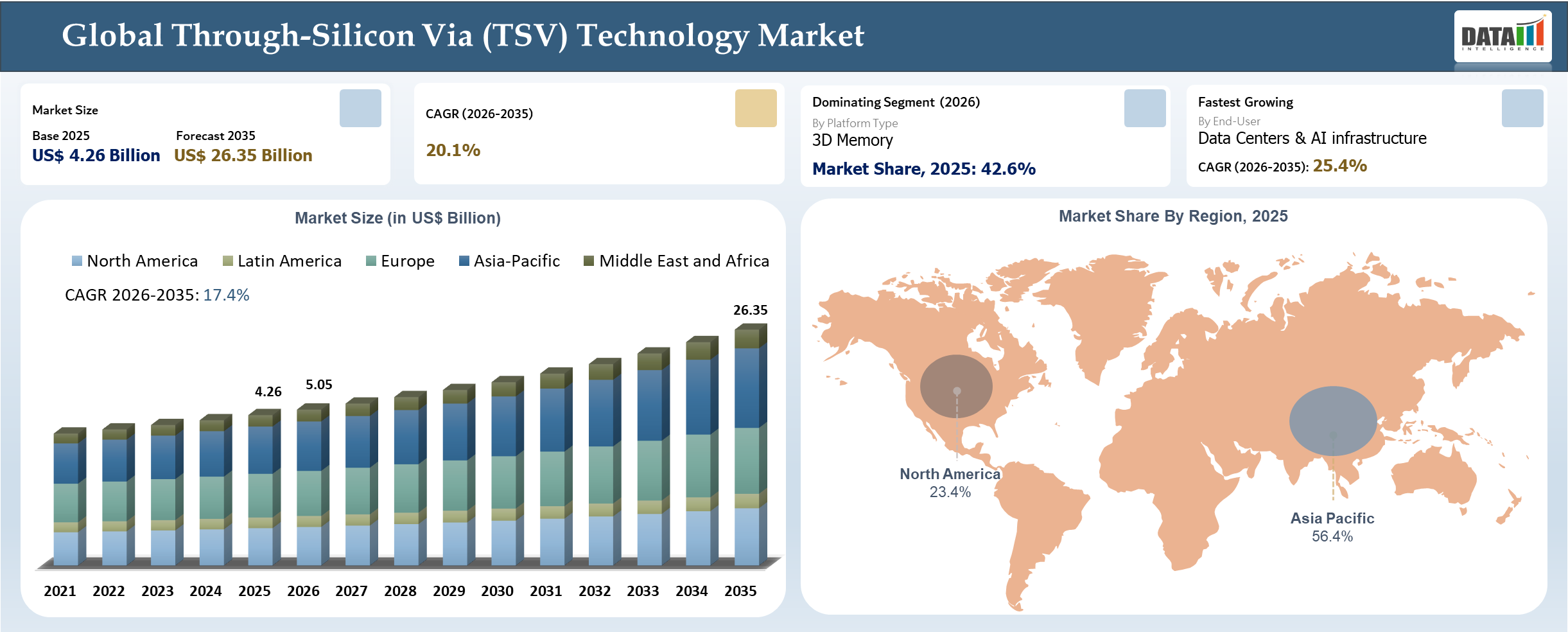
The global Through-Silicon Via (TSV) Technology market reached US$ 4.26 billion in 2025 and is expected to reach US$ 26.35 billion by 2035, growing with a CAGR of 20.1% during the forecast period 2026-2035. Use of TSVs in the packaging of ICs is increasingly becoming prominent as a major contributor in facilitating the development of semiconductor systems that feature high-performance and high miniaturization levels, following a growing demand within such fields as artificial intelligence, data center applications, 5G communications, and automotive engineering. Currently, the most popular form of IC packaging is 2.5D interposer packaging owing to its superior cost-effectiveness, scalability, and reliability, especially in the development of AI accelerators, with the fastest-growing one being 3D TSV packaging due to its enhanced bandwidth capability.
Through-Silicon Via (TSV) Technology Industry Trends and Strategic Insights
- HBM scaling is directly increasing TSV intensity, with each HBM stack integrating thousands of TSVs and next-generation configurations exceeding 100,000 TSV connections per stack, making memory architecture the primary driver of TSV consumption.
- AI accelerators are structurally dependent on TSV-enabled architectures, as modern processors integrate multiple HBM stacks delivering up to 3-5 TB/s bandwidth, positioning TSV density as a key determinant of system-level performance.
- TSV density is rising with each technology node, driven by higher stack heights (12-layer and beyond) and increased power delivery requirements, with advanced designs incorporating significantly higher TSV counts to improve electrical performance and reduce voltage drop.
- Bandwidth scaling in HBM (approaching 1 TB/s per stack in HBM3E) is reinforcing TSV as a non-substitutable interconnect, ensuring sustained demand growth as AI workloads continue to expand in data centers and high-performance computing environments.
Market Scope
| Metrics | Details | |
| 2025 Market Size | US$ 4.26 Billion | |
| 2035 Projected Market Size | US$ 26.35 Billion | |
| CAGR (2026-2035) | 20.1% | |
| Largest Market | Asia-Pacific | |
| Fastest Growing Market | Asia-Pacific | |
| By Process Type | Via-First TSV, Via-Middle TSV and Via-Last TSV | |
| By Platform Type | 3D Memory, 2.5D Interposer, 3D Logic and Sensor-Embedded | |
| By Application | Memory Applications, Compute / Packaging Applications, Sensor Applications and Others | |
| By End-User | Data Centers & AI infrastructure, Consumer Electronics, Automotive, Industrial & IoT, Healthcare and Others | |
| By Integration | Wafer-to-Wafer (W2W), Die-to-Wafer (D2W) and Die-to-Die (D2D) | |
| By Material | Copper-filled TSV, Tungsten-filled TSV and Dielectric liners | |
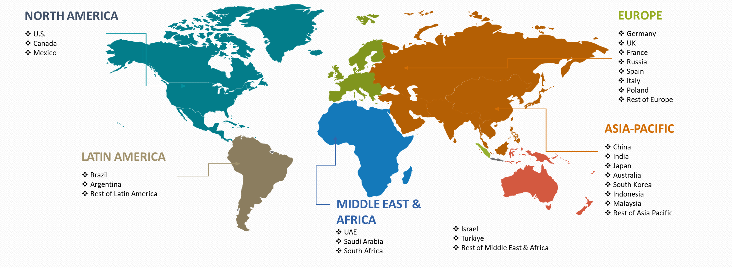
| By Region | North America | U.S., Canada, Mexico |
| Europe | Germany, UK, France, Spain, Italy, Poland | |
| Asia-Pacific | China, India, Japan, Australia, South Korea, Indonesia, Malaysia | |
| Latin America | Brazil, Argentina | |
| Middle East and Africa | UAE, Saudi Arabia, South Africa, Israel, Turkiye | |
| Report Insights Covered | Competitive Landscape Analysis, Company Profile Analysis, Market Size, Share, Growth | |
Disruption Analysis
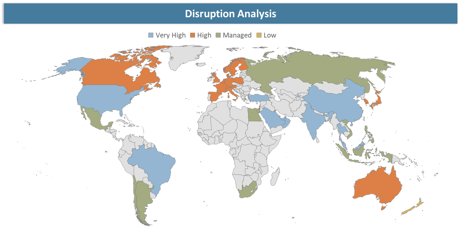
Advanced Packaging Capacity Constraints Emerging as a Structural Bottleneck in TSV Deployment
The application of TSV technology is hindered by the lack of advanced packaging infrastructure, especially for the integration of HBM and 2.5D interposer-based structures in AI accelerators. The production of TSV packages involves complex procedures, including wafer bonding, interposer fabrication, and alignment that have slower scaling cycles than wafer processing. The fast expansion of AI computations has generated an imbalance between supply and demand, causing increased delays and favoring select customers.
Due to capacity constraints, packaging is becoming a strategic bottleneck in the semiconductor industry’s value chain. For instance, key companies like TSMC and Samsung Electronics have been increasing their capacity in TSV packaging, whereas system designers are optimizing architectures to suit the existing capacity. The factors have made TSV packaging a key bottleneck for future AI/HPC solutions.
BCG Matrix: Company Evaluation
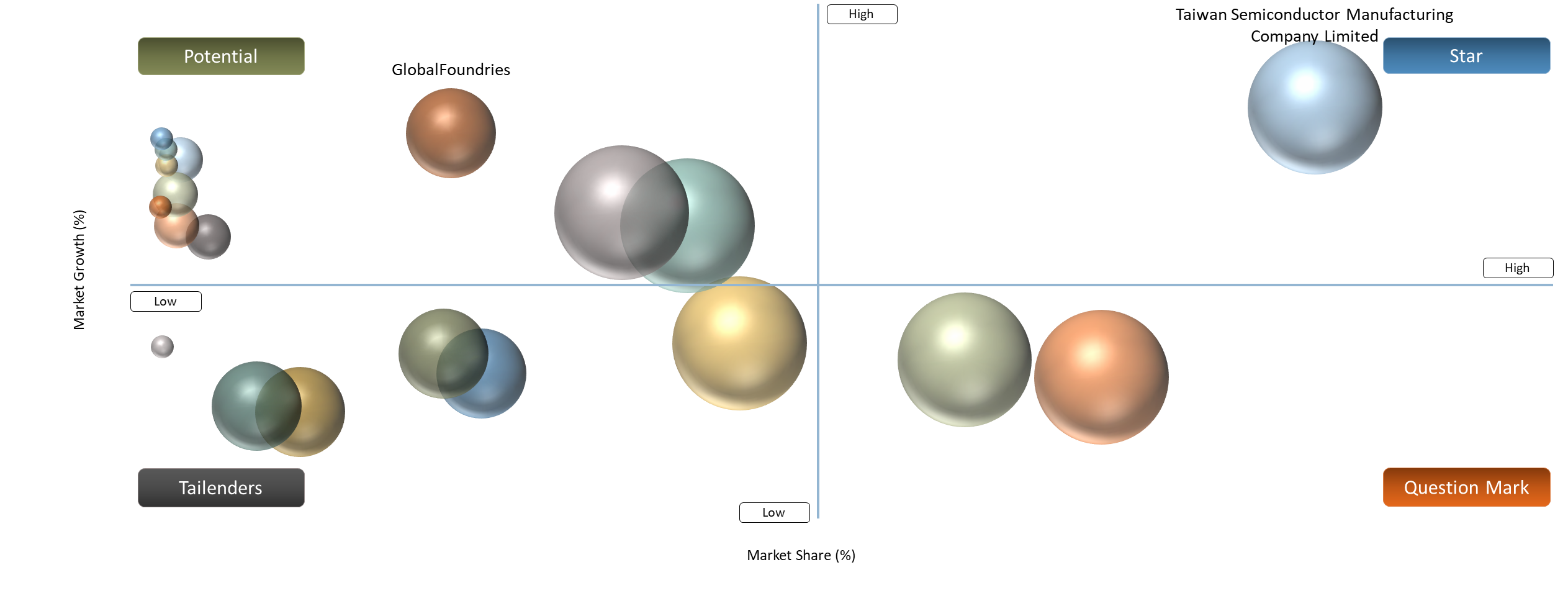
Leading players in the TSV market are based in the Star quadrant, driven by strong market share and direct exposure to high-growth AI and advanced packaging demand. Taiwan Semiconductor Manufacturing Company, Samsung Electronics, SK hynix, and Micron Technologies are considered leading players in the market owing to their market dominance in HBM and their advanced packaging technologies. Intel is also considered among such companies owing to its activities involving 3D packaging. Such companies have an advantage owing to substantial capital investments, technological supremacy, and direct impact on AI-related demand.
Companies classified under question marks include Amkor Technology and Powertech Technology Inc., which indicate their higher dependency on TSV growth coupled with lesser control in the market than foundries and memory vendors. The company, Applied Materials, is located in-between Star and Potential, owing to its crucial contribution to enabling technology rather than being involved directly in TSV manufacturing. The companies, including GlobalFoundries, United Microelectronics Corporation, STMicroelectronics, Nanya Technology, and ams-OSRAM, are considered Tailenders or Potential depending upon their low exposure to TSV high-growth sectors such as HBM.
Market Dynamics
Driver Impact Analysis
| Driver | Market Growth Impact (%) | Demand Concentration | Impacted Use Case | Strategic Impact |
| AI Infrastructure Scaling through HBM Integration | 2.5% | Concentrated in hyperscale data centers and AI clusters across North America and Asia-Pacific | AI accelerators with HBM-integrated GPUs/ASICs | Significantly increases TSV density per device and reinforces premium advanced packaging demand |
| Transition to 2.5D and 3D Advanced Packaging Architectures | 2.0% | Primarily centered in Taiwan and South Korea manufacturing ecosystems | 2.5D interposer-based logic-memory integration | Establishes TSV as a core interconnect technology, replacing conventional packaging approaches |
| Increasing Memory Bandwidth Requirements in AI Workloads | 1.8% | Global demand led by cloud service providers and AI infrastructure operators | High-bandwidth AI training and inference systems | Positions TSV density as a critical determinant of system-level performance and efficiency |
| Adoption of Chiplet-Based Processor Architectures | 1.5% | Strong in design-driven markets such as the United States and Taiwan | Chiplet-based CPUs and GPUs | Enables modular system architectures requiring high-density interconnect solutions |
Acceleration of AI and High-Performance Computing Driving TSV Adoption
Rapid scaling of the AI infrastructure has led to a significant increase in demand for TSV technologies due to the use of HBM stacks in contemporary accelerators. In particular, each HBM stack consists of thousands of TSV structures, and there is more than one HBM stack in contemporary AI chips; therefore, the TSV density increases substantially. In addition, the scaling of TSV technologies, including the introduction of the CoWoS and I-Cube platforms used in advanced packaging from such companies as TSMC and Samsung Electronics, respectively, is contributing to an increase in the capacity for AI chips.
On the other hand, structural limitations have reinforced the strategic significance of TSV technology from the supply side perspective. For instance, memory providers like SK Hynix and Micron Technology have been allocating most of their capacity towards manufacturing memory chips for AI-based workloads, such as Hyperscale workloads. However, at the same time, the capability for performing advanced packaging tasks has been constrained, which makes the use of TSV-based integration technology a very important limitation in the adoption of AI-based hardware components.
Restraint Impact Analysis
| Restraint | Drag on Market Growth (%) | Primary Impact Area | Impacted Use Case | Strategic Impact |
| Advanced Packaging Capacity Constraints | 2.5% | OSAT and foundry packaging lines | HBM-integrated AI accelerators and 2.5D interposer packages | Limits the scalability of TSV-enabled AI and HBM deployment, creating supply bottlenecks |
| High Fabrication Complexity and Cost Structure | 2.2% | TSV process integration (etch, fill, thinning) | High-density 3D stacking and HBM production | Restricts adoption beyond high-value applications due to elevated manufacturing costs |
| Yield Losses and Defect Sensitivity in TSV Processes | 1.9% | Manufacturing yield and process control | Multi-die stacking and high TSV count architectures | Reduces production efficiency and increases cost per unit, impacting commercialization |
High Fabrication Complexity and Cost Constraints in TSV Integration
TSV technology adds a complicated and very sensitive process flow, involving DRIE, dielectric liners and barriers deposition, copper plating, wafer thinning, and backside via formation. It significantly complicates production compared to traditional packaging technology due to the fact that each step carries tight process tolerances; deviations can lead to defects such as voids, misalignment, or liner integrity issues, directly impacting yield. At high densities, like HBM and 3D IC technologies, where thousands of TSVs have to be created, the complexity is further increased because of high tolerance requirements and time cycles.
Higher cost levels are also contributed to by low initial yields, high capital intensity, and difficulties integrating front-end and back-end technologies. Advanced packaging systems for TSV technology entail considerable costs in terms of machinery and raw materials. Similarly, wafer thinning operations pose a risk of breakage and malfunction, leading to higher cost levels. Consequently, TSV technology is still susceptible to increased production costs, especially for volume consumer products.
Segmentation Analysis
The global Through-Silicon Via (TSV) Technology market is segmented based on Process Type, Platform Type, Application, End-User, Integration, Material and region.
High-Bandwidth Memory (HBM) Driving Dominant TSV Adoption in AI and HPC Architectures
High Bandwidth Memory is the most notable use case of Through Silicon Via technology and relies on it to achieve cutting-edge memory architectures needed in AI accelerators and other compute-intensive machines. Vertical stacking of DRAM dies in HBM with the help of TSV technology allows for achieving a significantly improved bandwidth-to-latency ratio in comparison with other types of memory chips. Currently, 4 to 8 HBM stacks are utilized per chip in AI processors, where 8 to 12 DRAM dies are used in each stack, making thousands of Through Silicon Vias necessary per stack. The kind of architecture has become vital for providing several terabytes of bandwidth per second in AI workloads. Market concentration further highlights adoption intensity, with SK hynix accounting for nearly 50% share in the HBM segment, followed by Samsung Electronics and Micron Technology, indicating strong alignment between TSV deployment and memory-led demand.
Adoption trends show the fast scalability path of this technology with HBM evolving from a specialized solution for HPC workloads to becoming a key component in the AI architecture. Industrial roadmaps demonstrate an increasing trend towards 12 and 16 layers of HBM with a substantial rise in TSV usage in every single part, proving the growing significance of this technology in upcoming solutions. In addition, there is an increasing demand for HBM from hyperscale data centers causing a steady increase in the production capabilities of HBM, which, however, is currently mostly dedicated to AI workloads. The evolution will drive TSV growth at both the single and system levels making memories a leading segment in the TSV market.
Geographical Penetration
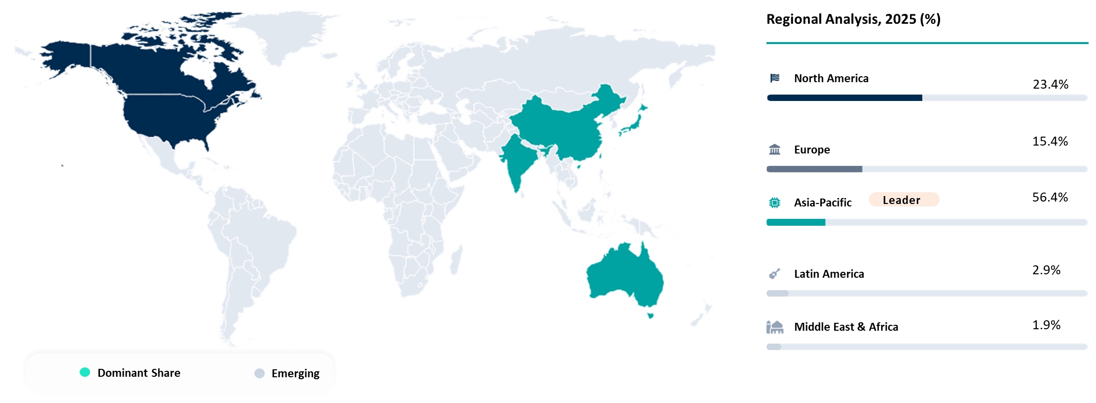
Asia-Pacific TSV Market Leadership Driven by Policy Support and Integrated Supply Chains
Asia-Pacific dominates the market for through-silicon vias due to the presence of a well-established semiconductor ecosystem backed by robust industrial policies and manufacturing scale. The implementation of national strategies focused on advanced packaging, memory fabrication, and resilience along the supply chain has played a significant role in accelerating the use of TSVs. Collaboration within the region ensures effective movement of goods from wafer fabrication in Taiwan, memory fabrication in South Korea, and semiconductor assembly in Southeast Asia, which is an efficient value chain. More importantly, Asia-Pacific is the largest provider of semiconductor packaging and test services in the world, making the region the leading adopter of TSV technology.
Industrial capabilities in the Asia-Pacific regions are additionally reinforced by the presence of an efficient workforce, advanced infrastructure, and close vicinity to centers of intensive electronics fabrication. A major portion of the capability in advanced semiconductor fabrication comes from Taiwan, thus making it the upstream foundation for TSV-based packaging solutions. The constant development of state-of-the-art packaging facilities alongside incentives provided by the government ensures that adoption of 2.5D and 3D integration technologies proceeds at a rapid pace.
Taiwan Strengthening TSV Leadership Through Advanced Packaging and Export-Oriented Manufacturing
Taiwan holds a dominant place in the development of TSV technology because of its advanced semiconductor manufacturing and package integration. The Taiwanese government's active support in the realm of semiconductors, along with its foundry industry, helps in making improvements in TSV-based technologies. Some major companies like TSMC and ASE Technology Holding contribute to Taiwan’s capability in packaging systems using interposers. The export-oriented manufacturing business makes Taiwan an important link in global semiconductor industry trade for AI accelerators and HPC systems.
Taiwan continues to invest in its advanced packaging facilities and logistical systems to solidify its leadership. Platforms that promote industry collaboration and large-scale events involving semiconductors help develop the ecosystem as well as facilitate information sharing related to new innovations. The integration of design, manufacturing, and packaging helps in the scaling up of TSV solutions to meet international demands.
South Korea Driving TSV Adoption Through Memory Leadership and Strategic Policy Initiatives
South Korea is an important player in expanding the market for TSV due to its dominance in the manufacturing of memory components, especially in high-speed memory devices where TSV technology is crucial for the 3D stacking process. Government-backed initiatives, including the implementation of policies like the K-CHIPS Act, which offers considerable tax breaks and R&D assistance. Exporting memory devices ensures that South Korea becomes an essential exporter to the global market for AI and HPC technologies.
Dominance in HBM production by corporations such as SK hynix and Samsung Electronics contributes to establishing the nation as a, major source of volume for TSVs. Constant increases in capacity levels in addition to investments made through national policies in AI and semiconductor advancements ensure the continued growth in the use of TSVs. The integration of memory manufacturing with high-tech applications ensures that the nation plays a key role in the development of TSVs.
Competitive Landscape
- Market leaders for TSV technology include vertically integrated firms with robust expertise in advanced packaging, logic process technology, and memory integration. Leading firms include Taiwan Semiconductor Manufacturing Company, Samsung Electronics, and Intel, who remain market leaders due to their dominance in the 2.5D/3D packaging platform and synchronization with artificial intelligence demands. Large-scale use of TSV technology is facilitated by memory producers like SK hynix, Micron Technology, and Nanya Technology through the production of high-bandwidth memory.
- Supporting players in packaging and equipment categories have been crucial in facilitating the scaling process. For instance, Amkor Technology and Powertech Technology Inc. have been involved in contributing their advanced assembly and test solutions. Applied Materials is known for its key contributions in providing essential tools that are necessary for the fabrication of TSVs. GlobalFoundries, United Microelectronics Corporation, STMicroelectronics, and ams-OSRAM have their presence in selected areas. Competitiveness depends on having access to advanced packaging facilities and supporting TSV-based AI and HPC systems.
- Key players include Taiwan Semiconductor Manufacturing Company Limited, Samsung Electronics, Intel Corporation, GlobalFoundries, United Microelectronics Corporation, STMicroelectronics, SK hynix Inc., Micron Technology, Inc., Nanya Technology Corporation, Amkor Technology, Powertech Technology Inc., Applied Materials, Inc. and ams-OSRAM AG
Key Developments
- April 2026 - SEC developed an innovative X-ray based inspection solution for packages that employ TSV technology like HBM and 2.5D interposers. The system uses proprietary algorithms and selective CT to increase the speed of inspections considerably, lowering the inspection process of HBM from a few minutes to less than one minute. The accuracy is maintained at micron level and the inspection also helps in improving defect detection, yield management, and production scalability.
- December 2025 - Technology development in the TSV market focused on advancing design methodologies and multiphysics simulation for 3D IC integration, with emphasis on TSV pitch optimization, parasitic modeling, keep-out zone (KOZ) management, and thermo-mechanical reliability. With Cadence Design Systems and other platforms, the technology enhancements will help validate and lay out designs using TSV architecture, improving signal integrity, power efficiency, and reliability.
- May 2025 - ASE Technology Holding launched FOCoS-Bridge with TSV, a new advanced packaging technology aimed at improving the efficiency and energy savings in AI and high-performance computing applications. With TSV in FOCoS-Bridge technology, there is a shorter distance between connections, increased I/O capacity, and better heat dissipation, leading to 3× improvement in energy loss and lower resistance and inductance levels. It supports the expansion of ASE's VIPack technology offerings that can accommodate chiplets and HBM, which require higher bandwidth and power delivery capabilities in future semiconductors.
Why Choose DataM?
- Technological Innovations: Covers critical developments in TSV fabrication, including high-aspect-ratio etching, advanced electroplating, wafer thinning, and integration with 2.5D/3D packaging architectures. Focus includes how these innovations improve interconnect density, signal integrity, thermal performance, and enable next-generation HBM and chiplet-based designs.
- Product Performance & Market Positioning: Evaluates TSV-enabled solutions across HBM, interposer-based packaging, and 3D IC integration. Analysis benchmarks performance parameters such as bandwidth efficiency, power consumption, TSV density, and scalability across AI, HPC, and advanced semiconductor applications.
- Real-World Evidence: Highlights large-scale implementation of TSV technology in AI accelerators, high-bandwidth memory, and advanced packaging platforms. Demonstrates measurable outcomes such as improved data throughput, reduced latency, and enhanced system-level performance in data centers and high-performance computing environments.
- Market Updates & Industry Changes: Tracks key developments including expansion of advanced packaging capacity, evolution of HBM architectures, and integration of TSV with chiplet and heterogeneous design frameworks. Coverage includes adoption trends across major semiconductor manufacturing regions.
- Competitive Strategies: Analyzes how leading players strengthen their position through capacity expansion, technology innovation, and strategic collaborations across foundries, memory manufacturers, and OSAT providers. Focus includes partnerships, investments, and vertical integration strategies.
- Pricing & Market Access: Explains cost dynamics associated with TSV integration, including fabrication complexity, yield considerations, and pricing premiums in advanced packaging. Reviews how cost optimization and process efficiency influence market adoption across different application segments.
- Market Entry & Expansion: Identifies growth opportunities driven by AI infrastructure expansion, increasing demand for high-bandwidth memory, and the shift toward heterogeneous integration. Outlines strategic approaches for market entry, including targeting high-growth applications, building advanced packaging capabilities, and aligning with regional semiconductor ecosystems.
Target Audience
- Enterprises & Security Operations Teams: Large enterprises across BFSI, telecom, healthcare, retail, and manufacturing deploying NHI IAM solutions to secure machine identities across cloud, DevOps, and AI-driven environments. Focus areas include strengthening machine identity security, improving visibility of service accounts and APIs, and enforcing granular non human access control to reduce credential-based risks and support Zero Trust architectures.
- Managed Security Service Providers (MSSPs) & IT Service Firms: Service providers embedding NHI security into managed offerings, delivering identity discovery, continuous monitoring, and automated remediation. Emphasis is on strengthening client security posture, improving compliance, and enabling scalable identity governance across hybrid and multi-cloud environments.
- Cloud Service Providers & Hyperscalers: Organizations such as Amazon Web Services, Microsoft, and Google Cloud integrating native identity controls for workloads, APIs, and services. Focus includes enabling federated identities, token-based authentication, and policy-driven access across distributed cloud ecosystems.
- Identity Security & Cybersecurity Vendors: Companies including CyberArk, Saviynt, and HashiCorp developing platforms for secrets management, identity governance, and machine identity lifecycle management. These vendors are driving innovation in identity-centric security and platform consolidation.
- Investors & Private Equity Firms: Investment groups targeting high-growth opportunities in identity security, particularly in areas such as secrets management, identity discovery, and AI-driven governance. Interest is driven by rapid expansion of machine identities and increasing enterprise demand for identity-centric security solutions.
- Government & Regulatory Bodies: Public sector organizations establishing cybersecurity policies and compliance standards aligned with Zero Trust and identity-based security models. Focus includes enforcing governance over machine identities, enhancing national cyber resilience, and supporting secure digital infrastructure across critical sectors.