Solar Ingot and Wafer Market Size and Overview
The global solar ingot and wafer market was valued at approximately US$ 15.8 billion in 2025 and is projected to reach about US$ 29.7 billion by 2035, expanding at an estimated CAGR of approximately 6.5% during 2026-2035. Volume growth is stronger than value growth because aggressive capacity expansion and productivity gains continue to pressure wafer ASPs.
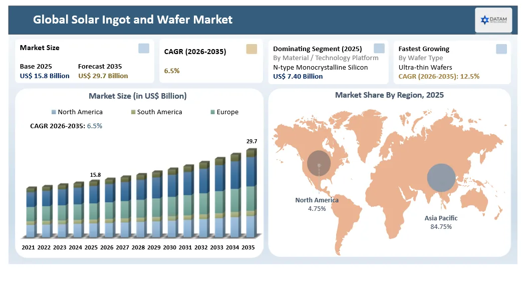
The market entered 2026 with persistent oversupply, low product prices and accelerated technology migration toward n-type monocrystalline wafers. LONGi reported Q1 2026 revenue of CNY 11.19 billion and maintained a full-year wafer shipment target of about 100 GW. JinkoSolar reported Q1 2026 revenue of RMB 12.25 billion and expects integrated production capacity of about 100 GW by year-end 2026.
| Metric | Details |
| 2025 Market Size | US$ 15.8 Billion |
| 2035 Projected Market Size | US$ 29.7 Billion |
| CAGR (2026-2035) | 6.5% |
| Largest Wafer Type | N-type Monocrystalline |
| Dominant Region | Asia-Pacific |
| Fastest-Growing Region | Middle East & Africa / India-led South Asia |
| Key Demand Engine | TOPCon, HJT and Back-Contact Cell Capacity |
| Core Market Challenge | Oversupply, low utilization and wafer price pressure |
Solar Ingot and Wafer Market Key Takeaways
- N-type monocrystalline wafers are gaining share as TOPCon, HJT and back-contact cell architectures expand across utility and distributed solar markets.
- Wafer dimensions are evolving beyond standard square formats toward larger and rectangular geometries that improve module power density and manufacturing utilization.
- Diamond-wire slicing, thinner wafers and reduced kerf loss are central to lowering silicon consumption per watt and improving unit economics.
- China remains the dominant global manufacturing base, while India, the United States, Southeast Asia and the Middle East are encouraging localized PV supply chains.
- Oversupply and low utilization remain major constraints, forcing producers to prioritize cost leadership, inventory discipline and technology differentiation.
- Buyer decisions increasingly emphasize wafer thickness, breakage rate, resistivity distribution, oxygen content, surface quality, dimensions and compatibility with next-generation cells.
- The ecosystem is tightly coupled across polysilicon, quartz crucibles, crystal-pulling equipment, diamond wire, slicing tools, wafer producers, cell manufacturers and module makers.
- The market ecosystem is tightly coupled across EDA, wafer fabrication, wafering equipment, crystal growth processes, wafers, consumables, OSATs, wafer suppliers and end-device designers.
Solar Ingot and Wafer Industry Trends and Strategic Insights
- The industry is transitioning rapidly from p-type to n-type monocrystalline wafers. TOPCon remains the largest near-term demand engine, while HJT and back-contact architectures require tighter wafer quality and thickness control.
- Manufacturers are pushing thinner wafers to reduce silicon usage while maintaining mechanical strength. Better crystal quality, optimized pulling speeds, improved thermal fields and lower-kerf slicing are therefore key competitive levers.
- Wafer formats are becoming more diverse. M10-class 182 mm wafers remain important, while G12-class 210 mm and rectangular formats are used to increase module power and optimize container, tracker and system dimensions.
- Persistent overcapacity is compressing margins and increasing consolidation pressure. Producers with captive polysilicon, low-cost energy, efficient pullers and strong downstream cell/module integration have structural advantages.
- Supply-chain resilience is encouraging capacity outside China, but new entrants must overcome scale, yield, technology and cost disadvantages against established Asian producers.
- Policy support through domestic manufacturing incentives, trade measures and local-content programs is reshaping where future ingot and wafer capacity is considered.
Solar Ingot and Wafer Market Scope
| Metrics | Details |
| By Ingot Type | Monocrystalline Silicon; Multicrystalline Silicon; Continuous / Advanced Crystal Growth; Specialty / High-Purity |
| By Wafer Type | N-type; P-type; Ultra-thin; Other |
| By Wafer Size | M10 / 182 mm; G12 / 210 mm; Rectangular / Large Format; Other |
| By Manufacturing Process | Czochralski; Continuous Czochralski; Directional Solidification; Diamond-Wire Slicing & Advanced Kerf Reduction |
| By Cell Technology | TOPCon; HJT; Back Contact; PERC & Other |
| By Application | Utility-Scale; Commercial & Industrial; Residential; Distributed & Off-Grid; Specialty PV |
| By Business Model | Vertically Integrated / Captive; Merchant Wafer Supply; Long-Term Strategic Supply; Contract / Toll Manufacturing |
| By Material / Technology Platform | Solar-Grade Polysilicon; N-type Mono-Si; P-type Mono-Si; Ultra-thin / Low-Kerf Technology |
| By Region | North America; Europe; Asia-Pacific; South America; Middle East & Africa |
Why does this report matter in 2026?
The year 2026 is pivotal because the solar wafer industry is simultaneously dealing with oversupply, rapid n-type conversion, thinner silicon, rectangular formats and expanding localization policies. Procurement teams and investors need to separate nominal capacity from economically viable, technology-compatible output.
The report matters because upstream wafer competitiveness is determined by more than nameplate capacity. Crystal quality, electricity cost, polysilicon sourcing, pulling productivity, slicing yield, breakage, inventory management and downstream cell compatibility determine sustainable margins and bankability.
Solar Ingot and Wafer Market White Space & Investment Opportunities
- High-efficiency n-type ingot and wafer capacity optimized for TOPCon, HJT and back-contact cells.
- Ultra-thin wafer platforms that reduce silicon grams per watt without raising breakage rates.
- Rectangular and large-format wafers designed for higher module power and improved balance-of-system economics.
- Low-carbon wafer production using renewable electricity, recycled silicon and traceable carbon accounting.
- Localized ingot and wafer capacity in India, the U.S., Southeast Asia and the Middle East where downstream cell/module capacity is expanding.
- Advanced crystal-growth controls, AI-enabled process optimization, diamond-wire technology and wafer inspection that raise yield and reduce kerf loss.
Solar Ingot and Wafer Future Market Transformation
By 2035, the market is expected to be dominated by high-purity n-type monocrystalline wafers, thinner silicon, larger or rectangular formats and highly automated crystal-growth and slicing lines. Technology competition will focus on cost per watt, material efficiency, carbon intensity and cell-conversion compatibility.
Business models will continue to polarize between vertically integrated solar manufacturers and specialized merchant wafer suppliers. Long-term strategic agreements, regional manufacturing partnerships and co-location with cell plants will become more important where trade rules and logistics add friction.
Solar Ingot and Wafer Market Buyer Decision-Making Criteria
Buyers prioritize wafer type, resistivity, minority-carrier lifetime, thickness, total thickness variation, oxygen and carbon content, geometric accuracy, surface quality, breakage rate, cell-efficiency performance, supplier scale, delivery reliability, traceability and price per piece or per watt.
Solar Ingot and Wafer Market Economic & Investment Analysis
Economics are shaped by polysilicon input cost, electricity, crucible life, crystal-growth productivity, ingot yield, slicing throughput, diamond-wire consumption, kerf loss, wafer breakage and utilization. In an oversupplied market, small yield improvements can materially change cash cost and competitiveness.
Investment is shifting toward advanced n-type capacity, line upgrades for thinner and rectangular wafers, automation, low-carbon power sourcing and selective geographic diversification rather than indiscriminate greenfield expansion.
Solar Ingot and Wafer Investment Trends in the Market
- Foundries and OSATs are expanding solar ingot and wafer manufacturing and advanced wafer manufacturing capacity near major wafer-fab clusters.
- Memory suppliers are scaling high-efficiency n-type wafer stack height, bandwidth and advanced wafering while aligning capacity with advanced processor roadmaps.
- Equipment vendors are investing in wafer wafering, thinning, deposition, inspection and inspection for tighter interconnect pitches.
- Substrate and wafer suppliers are pursuing larger formats, improved warpage control and glass-based alternatives.
- Partnerships increasingly link foundries, OSATs, equipment vendors and chip designers to qualify complete advanced wafer manufacturing flows.
Strategic Indicators for Solar Ingot and Wafer Market
High Regulation Impact
Export controls, solar PV incentives, technology-transfer rules and supply-chain security policies influence where solar ingot and wafer manufacturing tools, processes and leading-edge products can be manufactured or sold.
High Investment Activity
Solar Ingot and Wafer are attracting substantial capital across solar ingot and wafer manufacturing fabs, high-efficiency n-type wafer lines, advanced wafering equipment, consumables, inspection and thermal solutions.
Supply Chain Disruption
Concentration in solar ingot and wafer manufacturing capacity, high-efficiency n-type wafer, consumables and specialized equipment creates allocation risk and can delay high-value solar PV programs.
Pricing Volatility
Pricing varies with wafer count, stack height, interconnect density, wafer size, consumable availability, yield and qualification requirements. high-efficiency solar PV supply chains command a premium over conventional manufacturing.
Procurement Pressure
Buyers face pressure to reserve solar ingot and wafer manufacturing slots, secure high-efficiency n-type wafer and consumables and qualify alternate assembly sites without compromising yield or reliability.
New Technology Adoption
Hybrid wafering, TGVs, next-generation wafers, backside power delivery, high-efficiency n-type wafer4, wafer-to-wafer stacking and thermal-aware wafer process design are changing integration strategies.
Regional Expansion Opportunity
Asia-Pacific remains the manufacturing center, while North America, Europe and Japan are expanding domestic solar ingot and wafer manufacturing capacity and solar PV ecosystem resilience.
Government Policy Support
CHIPS-style incentives and national solar PV strategies increasingly include solar ingot and wafer manufacturing, consumables, R&D centers and PV manufacturing pilot lines.
Pricing Intelligence
Pricing is shifting from simple PV supply chain cost toward system-level value, including bandwidth, power savings, yield, PV supply chain area and time-to-market benefits.
Disruption Analysis of Solar Ingot and Wafer Market
The market is being disrupted by advanced wafering, next-generation wafers, high-efficiency n-type wafer, large silicon and glass wafers and foundry-integrated manufacturing. These shifts move value toward manufacturing platforms that can deliver wafer-scale precision, high yield and reliable thermal performance.
Solar Ingot and Wafer Market BCG Matrix: Company Evaluation
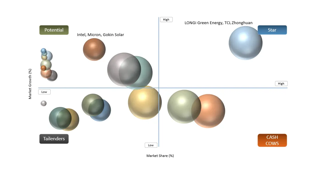
STAR
LONGi Green Energy, TCL Zhonghuan, JinkoSolar and JA Solar occupy the Star category because they combine very large crystal-growth and wafer capacity with integrated downstream cell and module demand. Their scale, technology roadmaps and customer access support leadership despite severe industry price pressure.
POTENTIAL
Intel, Micron, Gokin Solar, Besi, Hoyuan Green Energy and other equipment/material specialists remain high-potential participants as advanced wafering, high-efficiency n-type wafer and domestic solar ingot and wafer manufacturing investment expand.
Solar Ingot and Wafer Market Dynamics
Driver Impact Analysis
| Driver | Market Growth Impact | Demand Concentration | Impacted Use Case | Strategic Impact |
| N-type cell conversion | Very High | TOPCon, HJT and BC ecosystems | N-type monocrystalline wafers | Raises demand for tighter resistivity and material quality |
| Thinner wafers and kerf reduction | Very High | All high-volume cell manufacturing | Ultra-thin wafers | Reduces silicon grams per watt and lowers cost |
| Global PV installation growth | High | Utility, C&I and residential solar | All wafer formats | Expands baseline wafer volume demand |
| Localization policies | High | India, U.S., Southeast Asia, Middle East | Regional ingot and wafer capacity | Creates new capacity opportunities outside China |
Driver: high-efficiency solar, high-efficiency n-type wafer and Next-generation wafer Adoption Accelerating Advanced Wafer Manufacturing
The primary driver is the need to move more data between cell and wafer while controlling power and PV supply chain footprint. AI accelerators and HPC systems are adopting high-efficiency n-type wafer, large wafers and multi-wafer architectures, while smartphones, automotive systems and sensors use vertical integration to increase functionality within constrained form factors.
Restraint Impact Analysis
| Restraint | Drag on Growth | Primary Impact Area | Impacted Use Case | Strategic Impact |
| Industry overcapacity | Very High | China-led wafer supply | Merchant wafer sales | Suppresses utilization, pricing and margins |
| Wafer price volatility | Very High | All manufacturers | Spot and short-term procurement | Raises inventory and working-capital risk |
| Technology transition risk | High | P-type and older formats | Legacy capacity | Can strand equipment and reduce asset returns |
| Trade and localization barriers | Medium-High | Cross-border supply chains | Regional procurement | Increases qualification, logistics and compliance costs |
Restraint: Structural Oversupply, Price Pressure and Technology Obsolescence
Rapid capacity expansion has created a persistent supply-demand imbalance. Low utilization and wafer ASP pressure reduce returns on newer lines, while the transition toward n-type, thinner and rectangular formats can strand older p-type or fixed-format equipment. Manufacturers therefore face simultaneous cost, utilization and technology-upgrade pressures.
Solar Ingot and Wafer Market Segment Analysis
The global Solar Ingot and Wafer market is segmented based on Ingot Type, Wafer Type, Wafer Size, Manufacturing Process, Application, end-use industry, Business Model, material/technology platform, and region.
By Ingot Type
Monocrystalline Silicon Ingots Will Continue to Lead Market Value
silicon wafer stacked ICs remain the largest integration category because vertically stacked wafer, sensors and cell-wafer systems are already used at commercial scale. Monolithic advanced and finer-pitch heterogeneous approaches are expected to grow faster as advanced wafering improves density, power efficiency and PV supply chain-level performance.
By Wafer Type
P-type Wafers Will Record the Fastest Technology Growth
crystal growths remain foundational for many silicon wafer stacks, especially high-efficiency n-type wafer and mature wafer-level integration. Hybrid wafering is expected to gain share because direct copper-to-copper connections can deliver much finer pitch, lower parasitics and higher bandwidth density than conventional legacy slicing methods.
By Wafer Size
M10 / 182 mm Wafers Will Remain the Largest Product Segment
advanced wafer is the largest value pool because high-efficiency n-type wafer, stacked DRAM and advanced NAND rely on vertical architectures to increase capacity and bandwidth. Logic, image sensors, MEMS and heterogeneous photonic/RF integration expand the addressable market beyond wafer.
By Manufacturing Process
Czochralski (CZ) Crystal Growth and Next-Generation Wafers Integration Will Gain Share Rapidly
High-performance systems increasingly combine known-good compute, I/O and wafer wafers in one PV supply chain. Die-to-wafer flows offer flexibility in mixing wafer sizes and process nodes, while wafer-to-wafer wafering remains attractive where wafer dimensions and yields are closely matched.
By Application
AI / HPC and Data Centers Will Lead Application Growth
AI accelerators, CPUs, networking devices and high-efficiency n-type wafer-rich systems require extremely high wafer-to-wafer bandwidth and PV supply chain density. This makes data centers the strongest value-growth application, while smartphones, automotive electronics, imaging and edge devices broaden unit demand.
By End Use Industry
Utility-Scale Solar Will Continue to Dominate
Data centers, networking equipment, cloud infrastructure and telecom systems account for a large share of premium Solar Ingot and Wafer demand. Consumer electronics and automotive applications are also expanding as more processing, sensing and wafer are integrated into smaller PV supply chains.
Solar Ingot and Wafer Market Geographical Penetration
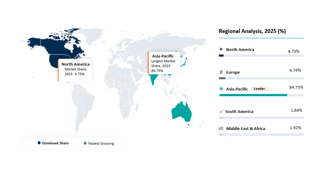
U.S. Solar Ingot and Wafer Market Landscape
The U.S. is a major market for Solar Ingot and Wafer design, equipment and advanced-compute demand, led by solar PV designers, hyperscalers, Intel, Hoyuan Green Energy, KLA and expanding domestic manufacturing investments. Policy incentives are encouraging more solar ingot and wafer manufacturing and consumable capacity onshore.
China Solar Ingot and Wafer Market Trends
China is expanding domestic solar ingot and wafer manufacturing, wafer, next-generation wafer and solar PV equipment capability while remaining a major electronics manufacturing market. Export controls constrain access to some leading-edge tools and technologies, increasing emphasis on localized supply chains.
Japan Solar Ingot and Wafer Market Outlook
Japan is strengthening solar PV manufacturing, advanced consumables, wafering materials and equipment through public-private investment. Its leadership in materials, precision equipment, automotive electronics and image sensors creates important advanced wafer manufacturing opportunities.
Germany Solar Ingot and Wafer Market Outlook
Germany combines automotive electronics, industrial automation, solar PV equipment and European research infrastructure. Growth opportunities center on power-efficient advanced PV manufacturing, sensors, automotive compute and EU-backed manufacturing R&D.
Middle East Solar Ingot and Wafer Market Outlook
The Middle East remains an emerging Solar Ingot and Wafer market, with Saudi Arabia and the UAE investing in data centers, solar PV ecosystem development and advanced technology partnerships. Near-term demand is primarily imported, while longer-term opportunities may develop in manufacturing, design services and regional electronics manufacturing.
Solar Ingot and Wafer Market Competitive Landscape
- Competition is structured around solar ingot and wafer manufacturing capacity, interconnect pitch, high-efficiency n-type wafer capability, advanced wafering know-how, wafer-level process integration, yield performance, geographic footprint and relationships with major fabless customers.
- LONGi and TCL Zhonghuan remain central to global monocrystalline ingot and wafer supply, while JinkoSolar, JA Solar and Trina Solar combine upstream wafer capacity with large downstream cell and module businesses. Gokin Solar and Shuangliang add merchant and integrated capacity that intensifies competition.
- Gokin Solar, Shuangliang Eco-Energy and Hoyuan Green Energy add merchant and integrated capacity, while Gaoce Technology strengthens the ecosystem through wafer slicing equipment and diamond-wire solutions.
- Market share can shift quickly because wafer products are relatively standardized and price competition is intense. Technology leadership therefore depends on n-type quality, thinner wafer capability, large or rectangular formats, yield, energy cost and customer qualification.
- Differentiation increasingly depends on crystal quality, low breakage, uniform resistivity, low oxygen and carbon content, slicing precision, silicon utilization, carbon intensity and the ability to support rapid cell-technology transitions.
Market Ecosystem Table
| Value Chain Sector | Representative Companies | Role in Solar Ingot and Wafer Market |
| Solar-Grade Polysilicon | Tongwei, GCL Technology, Daqo New Energy, Wacker Chemie | High-purity silicon feedstock for ingot pulling |
| Quartz Crucibles & Thermal Components | Ferrotec, Momentive, Heraeus and regional suppliers | Crucibles, graphite and hot-zone consumables for CZ growth |
| Crystal Growth Equipment | Jingsheng Mechanical & Electrical, NAURA and specialist suppliers | CZ pullers, thermal-field systems and automation |
| Diamond Wire & Slicing Equipment | Gaoce Technology, Metron, Meyer Burger and regional suppliers | Wafer slicing, wire consumables and kerf-loss reduction |
| Integrated Ingot & Wafer Leaders | LONGi, TCL Zhonghuan, Gokin Solar, JinkoSolar, JA Solar | Large-scale crystal growth and wafer manufacturing |
| Cell & Module Manufacturers | JinkoSolar, JA Solar, Trina Solar, LONGi, Tongwei | Downstream demand and wafer qualification |
| Regional New Entrants | Adani Solar, Waaree, Qcells and emerging U.S./Middle East projects | Localization and supply-chain diversification |
| Inspection / Metrology | KLA, Onto Innovation and specialist PV inspection vendors | Defect, geometry, thickness and surface-quality control |
| Logistics & Distribution | Specialty distributors, bonded warehouses and direct OEM channels | Wafer handling, storage and just-in-time delivery |
| Policy / Standards Ecosystem | IEA PVPS, IEC, national energy ministries and customs authorities | Standards, trade rules and industrial-policy support |
| Recycling & Circularity | Polysilicon reclaimers, kerf recycling and PV recycling firms | Silicon recovery, scrap recycling and carbon reduction |
Public Company Q1-Q2 2026 Performance Comparison
| Public Company | Reporting Period | Q1-Q2 2026 Performance | Growth Indicator | Factors Driving Solar Ingot & Wafer Exposure |
| LONGi Green Energy | Q1 2026 | CNY 11.19B revenue; company maintained ~100 GW 2026 wafer shipment target | Revenue pressured by low PV prices; technology mix improving | TaiRay wafers, n-type transition, BC ecosystem and scale manufacturing |
| TCL Zhonghuan | Q1-H1 2026 reporting window | Industry-leading ingot/wafer capacity; profitability remained pressured by sector oversupply | Focus shifted toward utilization, cost control and product mix | Large-format wafers, n-type products and merchant wafer scale |
| JinkoSolar | Q1 2026 | RMB 12.25B revenue; gross margin 8.3%; integrated capacity targeted at ~100 GW by end-2026 | Gross margin improved versus Q4 2025 and Q1 2025 | Integrated wafer-cell-module footprint and n-type Tiger Neo demand |
| JA Solar | Q1-H1 2026 reporting window | Large integrated PV manufacturing footprint; results remained exposed to low module and upstream prices | Technology transition and overseas mix are key variables | Captive ingot/wafer demand supporting TOPCon and high-efficiency products |
| Trina Solar | Q1-H1 2026 reporting window | Integrated solar manufacturing continued amid intense industry price competition | Global module demand supports captive wafer consumption | N-type cell/module roadmap, vertically integrated procurement and global expansion |
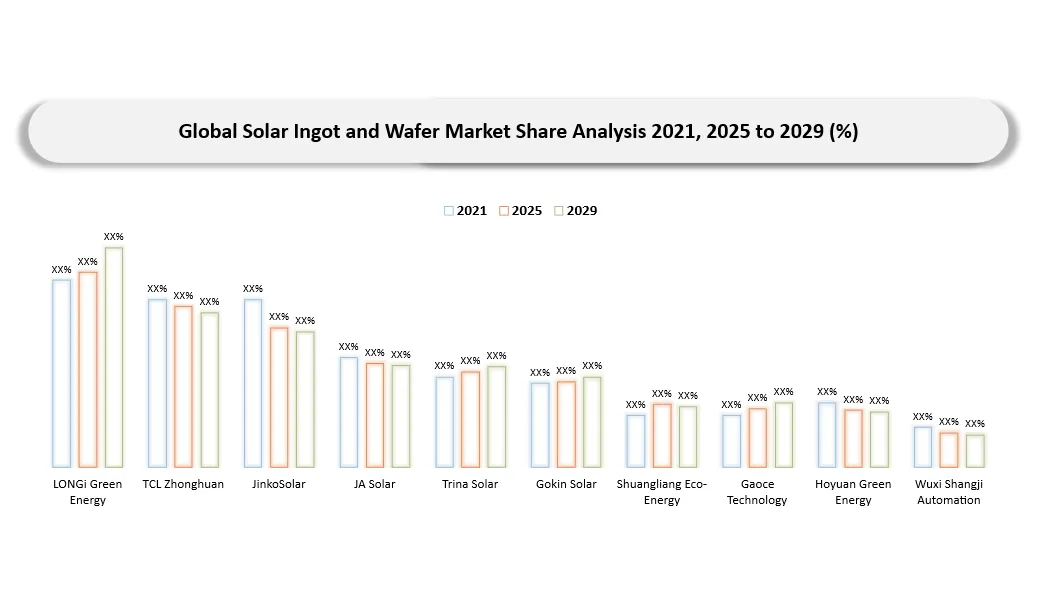
Key Companies
- LONGi Green Energy
- TCL Zhonghuan
- JinkoSolar
- JA Solar
- Trina Solar
- Gokin Solar
- Shuangliang Eco-Energy
- Gaoce Technology
- Hoyuan Green Energy
- Wuxi Shangji Automation
- Tongwei
- GCL Technology
- Daqo New Energy
- Ferrotec
- Sino-American Silicon Products
Company Profiles
LONGi Green Energy
LONGi is one of the world’s largest monocrystalline silicon ingot and wafer manufacturers. Its TaiRay wafer platform, large-scale crystal-pulling footprint and downstream cell/module operations provide strong exposure to n-type, back-contact and high-efficiency solar demand.
TCL Zhonghuan
TCL Zhonghuan is a major global producer of monocrystalline silicon ingots and wafers. The company has extensive large-format wafer capacity and serves both captive and merchant demand, with strategic emphasis on n-type products, cost reduction and manufacturing efficiency.
JinkoSolar
JinkoSolar operates an integrated wafer, cell and module platform. Upstream capacity supports its n-type product roadmap and provides captive demand visibility, while its global module business links wafer utilization to international solar installations.
JA Solar
JA Solar is a vertically integrated PV manufacturer with ingot and wafer capacity supporting its cell and module operations. Its upstream assets reduce procurement dependence and enable tighter coordination of wafer dimensions, thickness and cell technology.
Trina Solar
Trina Solar operates an integrated PV manufacturing platform with upstream silicon wafer exposure supporting its n-type cell and module roadmap. Its global manufacturing footprint and downstream demand provide captive consumption advantages, although sector-wide oversupply and low pricing continue to pressure upstream economics.
Gokin Solar
Gokin Solar is a specialist monocrystalline silicon ingot and wafer producer with substantial exposure to large-format and n-type products. Its competitiveness depends on high puller utilization, low electricity cost, slicing yield and disciplined capacity management.
Shuangliang Eco-Energy
Shuangliang Eco-Energy participates in monocrystalline silicon wafer manufacturing alongside its energy-efficiency and equipment businesses. The company’s wafer operations are exposed to n-type conversion, industry utilization and sharp upstream price cycles.
Hoyuan Green Energy
Hoyuan Green Energy combines monocrystalline silicon materials activities with equipment capabilities. Its positioning reflects the broader trend toward integrating crystal growth, wafering know-how and downstream customer relationships.
Daqo New Energy
Daqo New Energy is primarily a high-purity polysilicon producer rather than a wafer manufacturer. It is included because polysilicon pricing, purity and supply availability directly shape ingot and wafer cash costs, inventory decisions and production economics.
Additional Company Coverage
Additional profiles and benchmarking include Gaoce Technology, Wuxi Shangji Automation, Tongwei, GCL Technology, Ferrotec and Sino-American Silicon Products, reflecting the broader equipment, polysilicon, crystal-growth, wafering and materials ecosystem.
Solar Ingot and Wafer Market Major Pain Points
- Low utilization can magnify fixed costs across crystal-pulling and slicing lines, making disciplined capacity planning and operating efficiency essential.
- Thinner wafers lower silicon consumption but increase breakage risk and require tighter control of crystal quality, slicing conditions, handling and cell-line compatibility.
- Large and rectangular wafer formats require precise geometry, bow/warp control, robust logistics and coordinated downstream tooling changes.
- Manufacturing capacity remains heavily concentrated in China, creating trade, localization and supply-chain concentration risks for downstream markets.
- Quartz crucibles, diamond wire, high-purity polysilicon and low-cost electricity are critical inputs whose availability and pricing affect wafer cash cost.
- Rapid n-type technology migration can shorten the useful life of older p-type or fixed-format production assets.
- Qualification cycles for new wafer thicknesses, dimensions and material specifications can slow adoption despite compelling cost-per-watt benefits.
- Capital intensity remains high across crystal growth, thermal-field systems, slicing, automation, inspection and supporting utilities.
Solar Ingot and Wafer Market Recent Developments
- April 2026: LONGi reported Q1 2026 operating revenue of CNY 11.19 billion and maintained a full-year wafer shipment target of approximately 100 GW while highlighting continued industry price pressure and technology transition.
- 2026: Leading wafer producers continued prioritizing utilization, cost reduction, n-type conversion and inventory discipline as low wafer prices and excess capacity constrained profitability across the PV supply chain.
- 2026: Manufacturers accelerated rectangular wafer formats, thinner silicon, high-efficiency n-type products and localized supply-chain strategies to align with TOPCon, HJT and back-contact cell roadmaps.
- April 2026: JinkoSolar reported Q1 2026 revenue of RMB 12.25 billion and an 8.3% gross margin, with year-end integrated production capacity expected to reach approximately 100 GW.
- 2026: The industry continued migrating toward n-type wafers, thinner silicon and rectangular formats while producers focused on utilization, inventory reduction and cash-cost improvement.
- 2026: Policy-driven localization in India, the United States, Southeast Asia and the Middle East increased interest in non-China ingot and wafer capacity, although scale and cost competitiveness remain major barriers.
Analyst View / Opinion on Solar Ingot and Wafer Market
- Solar ingot and wafer manufacturing is a core upstream layer of the PV value chain. The market’s strategic importance is rising as cell architectures demand tighter material specifications while trade policies encourage more geographically diversified supply.
- Near-term leadership will be determined by n-type capability, utilization, wafer thickness, silicon consumption per watt, breakage rate, energy cost and downstream customer qualification. Longer term, carbon intensity and regional supply security will become more important.
- TOPCon will remain the largest near-term demand engine, while HJT and back-contact technologies should broaden requirements for high-quality n-type wafers and tighter thickness control.
- Ultra-thin wafering should become increasingly important because every reduction in wafer thickness lowers silicon use per watt, provided manufacturers can control breakage, bow, warp and downstream handling losses.
- Vertically integrated manufacturers retain advantages through captive demand and coordinated technology roadmaps, while merchant suppliers can win through scale, cost leadership, flexible product mix and strong customer qualification.
- Equipment, crucible, diamond-wire, inspection and process-control suppliers can capture value as manufacturers pursue higher throughput, thinner wafers and tighter quality specifications.
Solar Ingot and Wafer Market Target Audience
| INDUSTRY | WHO SHOULD BUY THIS REPORT? | REASON TO BUY THIS REPORT |
| Ingot & Wafer Manufacturers | Strategy, operations, sales and capacity-planning teams | Benchmark capacity, technology transition, wafer formats and regional demand. |
| Cell & Module Manufacturers | Procurement, technology and supply-chain teams | Assess wafer qualification, supplier risk, pricing and n-type availability. |
| Polysilicon Suppliers | Commercial and strategic-planning teams | Link silicon demand to wafer thickness, yields and PV installation growth. |
| Equipment & Consumables | Product, sales and business-development teams | Quantify demand for pullers, crucibles, diamond wire, slicing and inspection tools. |
| Investors & Lenders | Equity research, project finance and diligence teams | Evaluate oversupply, utilization, cost curves, technology risk and localization economics. |
| Governments & Trade Bowafers | Industrial-policy and energy-transition teams | Assess supply-chain concentration, localization needs and trade exposure. |
Why Choose DATAM?
- Data-driven insights combining company filings, wafer shipment guidance, capacity disclosures, polysilicon and wafer pricing, solar installation trends and country-level manufacturing policy.
- Post-purchase analyst consultations for market entry, competitive benchmarking, manufacturing strategy, equipment positioning and customer targeting.
- Annual report updates covering n-type conversion, wafer thickness, new formats, capacity additions, utilization, technology transitions and regional supply-chain shifts.
- Specialized focus on major PV manufacturing hubs, public incentives, trade barriers and regional ingot and wafer localization initiatives.
- Actionable analysis connecting wafer demand with polysilicon supply, electricity cost, crystal-growth productivity, slicing yield, cell-technology roadmaps and geopolitical constraints.
What DATAM Uniquely Provides
- Ten-year forecasts across ingot type, wafer type, wafer size, manufacturing process, cell technology, application, business model and material/technology platform.
- Technology-level analysis linking crystal growth, wafer thickness, resistivity, large-format and rectangular designs, slicing yield, kerf loss, breakage and cell compatibility.
- Competitive benchmarking of integrated PV manufacturers, merchant wafer suppliers, polysilicon producers and crystal-growth/wafering equipment companies.
- Public-company 2026 performance comparison tied directly to Solar Ingot and Wafer and solar ingot and wafer manufacturing growth drivers.
- Market ecosystem mapping from polysilicon and quartz crucibles through crystal growth, slicing, inspection, wafer manufacturers, cell producers and module companies.