

Semiconductor Ultrapure Water Treatment Market Size and Overview
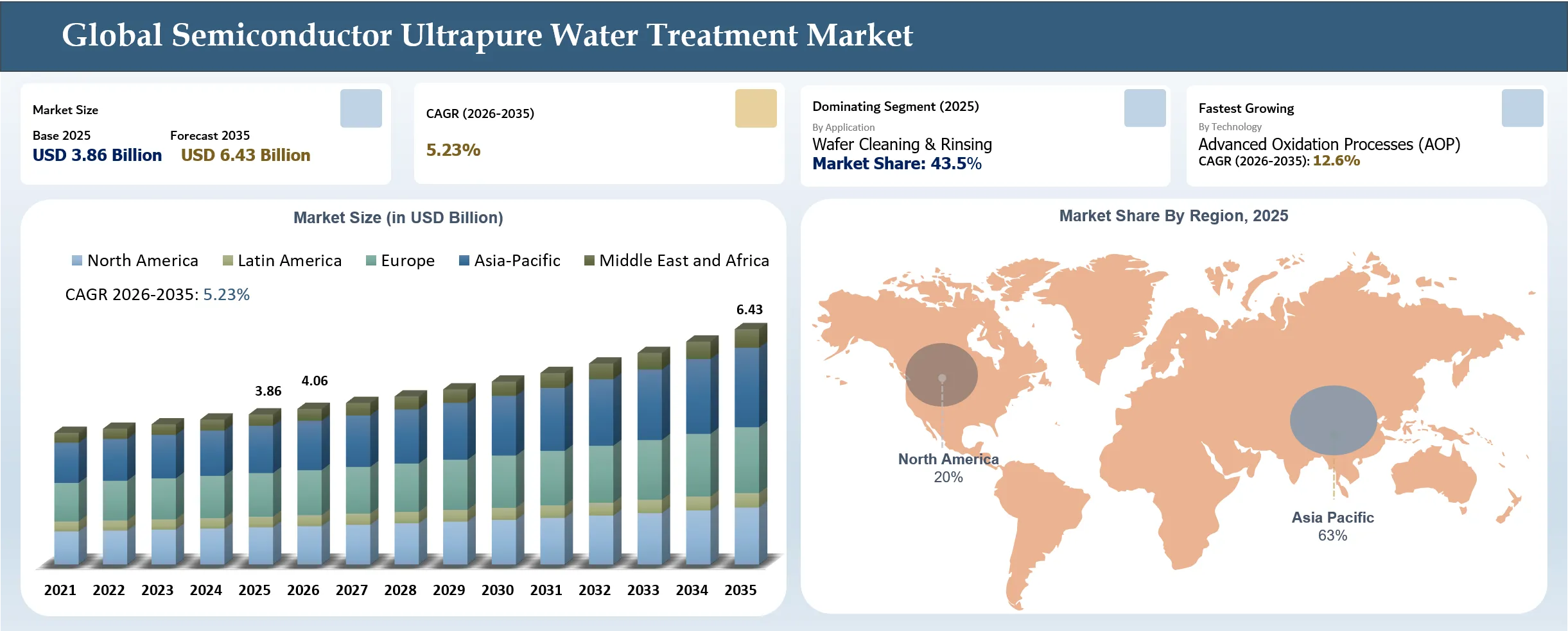
The global semiconductor ultrapure water treatment market reached USD 3.86 billion in 2025 and is expected to reach USD 6.43 billion by 2035, growing with a CAGR of 5.23% during the forecast period 2026-2035. The market demand is being reinforced by the increased production of semiconductors as well as by the water intensity of the sophisticated processes of fabrication. In March 2026, TSMC indicated the total water use of 151 million m³ in 2025, and the unit product water use was 153.3 liters per 12-inch wafer equivalent mask layer; TSMC used more than 23.53 million m³ of reclaimed water in 2025 with an 18% replacement rate in its Taiwan fabs. Powerchip Semiconductor Manufacturing Corporation (PSMC) indicated the ultrapure-water use of 10.006 million m³ in 2025, indicating the huge water treatment needs in the process of semiconductor fabrication. STMicroelectronics had a 51% water recycling rate in 2025, indicating the growing trend of water reuse and reclamation facilities in semiconductor manufacturing. In response to this trend, the demand for UPW generation, purification, polishing, distribution, monitoring, and reclamation systems is being intensified, particularly in the context of the expansion of advanced-node production and the reduction of freshwater use, and increasing water circularity. Companies such as TSMC, PSMC, STMicroelectronics, and Kurita Water Industries are enhancing their skills to recycle and manage ultrapure water in semiconductor factories.
The development of modern semiconductor fabrication plants is resulting in increased investments in ultrapure water and wastewater management systems. In June 2026, as per TopDaily, Hansung Clean Tech has signed a contract of KRW 22.2 billion (about USD 16 million) with Samsung E&A for the project “Pyeongtaek P5 Ph1 Ultrapure Water Complex Building Facility Construction A”. This contract comprises 11.09% of Hansung Clean Tech’s 2025 consolidated revenue, which is KRW 199.85139 billion (about USD 144.3 million). It will run until July 31, 2027, and involves building an ultra-pure water (UPW) supply facility for Samsung Electronics' semiconductor manufacturing infrastructure in Pyeongtaek P5 Ph1, which requires UPW for wafer cleaning. Previously, Hansung Clean Tech won a contract worth about KRW 16.4 billion (about USD 11.8 million) for the installation of a wastewater treatment system at the P5 Green Building.
White-Space Opportunities for Semiconductor Ultrapure Water Treatment, Driven by Dresden’s Semiconductor Water Infrastructure Investment
In June 2026, SachsenEnergie awarded HOCHTIEF a contract in the three-digit-million-euro range to design and build a new river-water treatment plant for Dresden’s semiconductor industry, as the total investment in the industrial-water supply system exceeds €300 million (approximately USD 351 million). The highest identified public investment is €150 million (approximately USD 176 million), jointly provided by the Free State of Saxony and the City of Dresden, including up to €100 million (approximately USD 117 million) from Saxony and €50 million (approximately USD 58.5 million) from Dresden, while SachsenEnergie finances a large share of the remaining investment. The largest investment area is the industrial-water treatment and supply system, comprising a high-capacity river-water treatment plant with capacity of up to 67,000 m³/day, while other major infrastructure includes approximately 22 km of industrial-water transport pipelines, storage facilities, pumping stations, and associated technical infrastructure. The system is scheduled to begin operation in 2030, when Dresden’s average industrial-water demand is projected to reach 165,000 m³/day, compared with 125,000 m³/day in 2025, while the semiconductor industry's share of water demand is expected to rise from 27% in 2025 to 45% in 2030. The investment is being driven by the expansion of Dresden’s semiconductor cluster, including Infineon and the ESMC project involving TSMC, Bosch, Infineon, and NXP, with ESMC’s semiconductor-fab investment reported at approximately €10 billion (USD 11.7 billion) and Infineon’s new Dresden production facility at approximately €5 billion (USD 5.85 billion).
The investment creates opportunities across industrial-water treatment, process-water infrastructure, water recycling, pumping, pipeline systems, filtration, process engineering, monitoring, and downstream semiconductor ultrapure-water treatment. HOCHTIEF is the most directly benefiting company from the announced water-infrastructure investment because it has been appointed general contractor for planning, permitting, construction, and turnkey delivery of the high-performance water-treatment plant, including civil construction, plant engineering, and process engineering. SachsenEnergie benefits as the project owner and future operator, while companies such as Bilfinger, STRABAG, VINCI, and Porr can benefit from civil engineering, construction, pipeline installation, and infrastructure development activities. KSB, Wilo, Sulzer, and Xylem are positioned across pumping, water conveyance, and fluid-management applications, while Veolia, Saur, Pentair, and Kurita Water Industries can benefit from industrial-water treatment, filtration, water recycling, and process-water solutions. DuPont, Toray Industries, and SUEZ have opportunities in membrane, reverse-osmosis, ion-exchange, and advanced water-treatment technologies. Downstream, Infineon, TSMC, Bosch, NXP Semiconductor, and ESMC benefit from a dedicated industrial-water supply that supports the expansion of semiconductor manufacturing in Dresden, creating further procurement opportunities for suppliers of advanced filtration, membrane systems, water recycling, monitoring, and ultrapure-water treatment equipment within individual fabs.
Semiconductor Ultrapure Water Treatment Market Key Takeaways
- The Asia-Pacific region dominated the global market by accounting for a 63% share in 2025. North America represented the second-largest regional market in 2025, contributing a 20% market share.
- Wafer cleaning and rinsing represents the largest application segment, holding a 43.5% market share in 2025. Advanced Oxidation Processes (AOP) is the fastest-growing technology segment, compound-growing at a CAGR of 12.6% from 2026 to 2035.
- Semiconductor fab investments in Dresden include ESMC’s €10 billion (USD 11.7 billion) facility and Infineon’s €5 billion (USD 5.85 billion) plant. The Dresden river-water supply infrastructure constructed by HOCHTIEF is scheduled to begin operations in 2030.
- Total investment for the industrial water supply system in Dresden, Germany, exceeds €300 million (USD 351 million). Public entities provided €150 million (USD 176 million), including €100 million (USD 116.7 million) from Saxony and €50 million (USD 58.3 million) from Dresden.
Semiconductor Ultrapure Water Treatment Market Industry Trends and Strategic Insight
- Shift toward closed-loop water management. Semiconductor manufacturers are moving beyond conventional UPW production toward integrated treatment, reclamation, and reuse architectures that recover contaminated process water and return it to fabrication operations.
- Increasing process sensitivity at leading-edge nodes is driving greater emphasis on ultra-low particles, metals, organics, dissolved gases, and other trace contaminants across the UPW distribution loop.
- Treatment suppliers are increasingly integrating wastewater segregation, advanced filtration, ultrafiltration, and polishing with UPW systems rather than treating water generation and wastewater management as separate infrastructure.
- New fab investments outside traditional semiconductor hubs are creating demand for locally engineered UPW generation, recycling, and maintenance capabilities, encouraging international water-treatment companies to establish regional partnerships and supply networks.
- Competitive differentiation is increasingly based on the combined ability to maintain semiconductor-grade purity while minimizing freshwater intake, chemical consumption, energy use, wastewater generation, and treatment-cycle losses.
Semiconductor Ultrapure Water Treatment Market Scope
| Metrics | Details | |
| 2025 Market Size | USD 3.86 Billion | |
| 2035 Projected Market Size | USD 6.43 Billion | |
| CAGR (2026-2035) | 5.23% | |
| Largest Market | Asia-Pacific | |
| Fastest Growing Market | North America | |
| By Treatment Stage | Pretreatment, Makeup Water Treatment, Primary Purification, Polishing, Point-of-Use Treatment, UPW Distribution, Others | |
| By Technology | Reverse Osmosis (RO), Ion Exchange, Electrodeionization (EDI), Ultrafiltration (UF), Microfiltration (MF), UV Oxidation, Membrane Degasification, Membrane Degasification, Advanced Oxidation Processes (AOP), Others | |
| By UPW Quality Requirement | Standard Semiconductor-Grade UPW, Advanced-Node UPW, Ultra-Low TOC UPW, Ultra-Low Metal UPW, Ultra-Low Particle UPW, Hot Ultrapure Water (HUPW), Others | |
| By Fab Type | Logic & Foundry Fabs, Memory Fabs, Analog & Power Semiconductor Fabs, Compound Semiconductor Fabs, MEMS & Sensor Fabs, Advanced Packaging Facilities, Others | |
| By Application | Wafer Cleaning & Rinsing, Photolithography, Etching, Chemical Mechanical Planarization (CMP), Deposition & Thin-Film Processing, Wafer Dicing & Back-End Processing, Others | |
| By End User | Semiconductor Foundries, Integrated Device Manufacturers (IDMs), Memory Manufacturers, Compound Semiconductor Manufacturers, MEMS & Sensor Manufacturers, Advanced Packaging & OSAT Providers, Semiconductor R&D Facilities, Others | |
| By Region | North America | U.S., Canada, Mexico |
| Europe | Germany, UK, France, Spain, Italy, Poland | |
| Asia-Pacific | China, India, Japan, Australia, South Korea, Indonesia, Malaysia | |
| Latin America | Brazil, Argentina | |
| Middle East and Africa | UAE, Saudi Arabia, South Africa, Israel, Türkiye | |
| Report Insights Covered | Competitive Landscape Analysis, Company Profile Analysis, Market Size, Share, Growth | |
Semiconductor Ultrapure Water Treatment Market Disruption Analysis
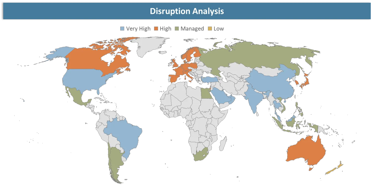
Shift Toward Closed-Loop UPW Systems Reshaping Semiconductor Water-Treatment Infrastructure
The disruption in the Semiconductor Ultrapure Water Treatment Market is mostly associated with the rapid shift toward closed-loop UPW systems, which involve the recycling of wastewater back into the semiconductor process instead of the extensive use of freshwater resources. Such developments have become very significant since processes involving wafer processing need continuous UPW flow. According to Infineon Technologies, the company withdraws 37.51 million m³ of water and uses 11.59 million m³ of ultrapure water in fiscal year 2025 while producing 16.32 million m³ of recycled water, demonstrating the increasing scale of water recovery within semiconductor manufacturing.
Also, Infineon is integrating wastewater recycling directly into semiconductor manufacture, with wastewater from production processes being collected, recycled using its own systems for recycling, and reused when possible. Significant amounts of wastewater are recycled back into the UPW process at its Tijuana and Dresden plants, and groundwater is recycled to create UPW at its Villach and Regensburg plants using reverse osmosis and ultrafiltration. Infineon has also developed recycling practices that have saved in excess of 16 million cubic meters of water in fiscal year 2025, surpassing its goal of recycling 15 million cubic meters annually. Thus, the market will be moving from simple make-up water treatment to UPW production, wastewater reuse, and water recycling systems.
Semiconductor Ultrapure Water Treatment Market BCG Matrix: Company Evaluation
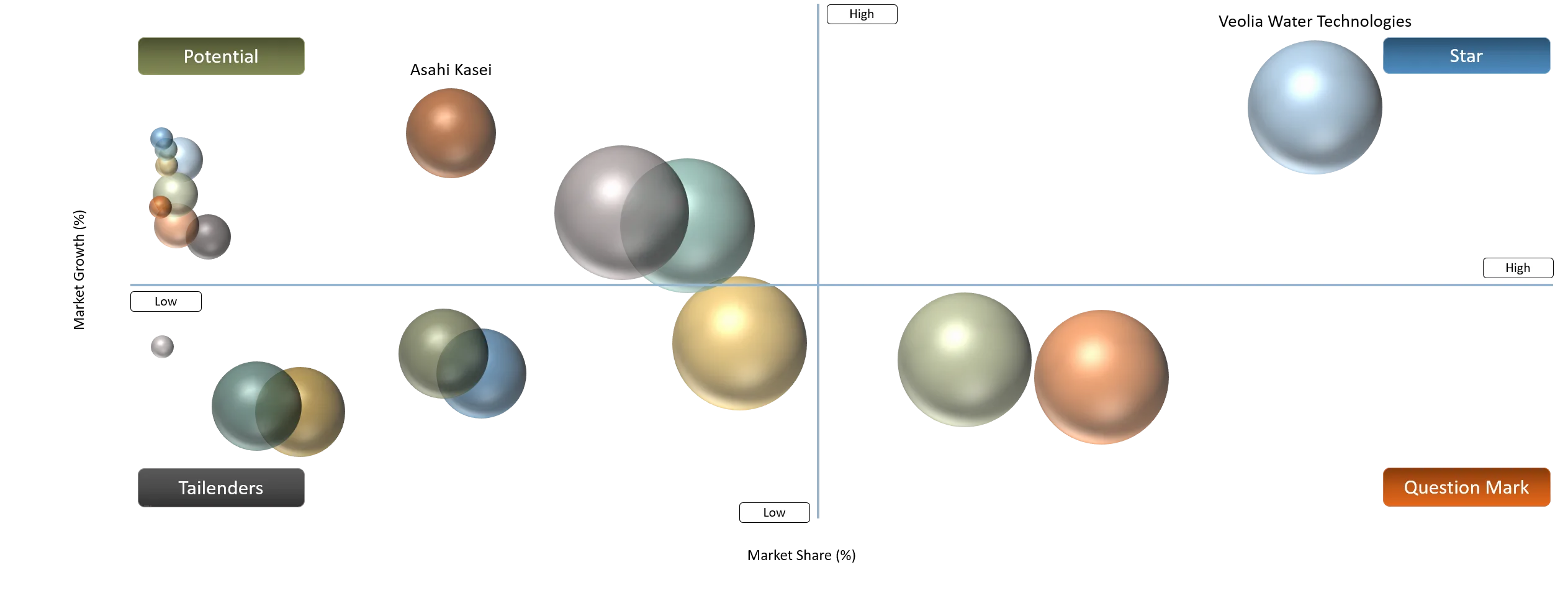
Stars include Veolia Water Technologies, Kurita Water Industries, Organo Corporation, and Nomura Micro Science because they have strong positions in semiconductor ultrapure-water treatment and provide integrated UPW generation, purification, wastewater reclamation, and water-management solutions for semiconductor fabs. Question Marks include Ecolab, Xylem, DuPont, and Toray Industries, as these companies possess established membrane, filtration, ion-exchange, water-treatment, and separation technologies that can address semiconductor UPW requirements but compete against specialized suppliers with deeper semiconductor-fab integration.
The Potential category includes Asahi Kasei, Pall Corporation, and Pentair, which benefit from demand for membrane filtration, microfiltration, ultrafiltration, contamination control, and high-purity water components used within semiconductor treatment systems. Tailenders include Aquatech International because its semiconductor water-treatment activities are comparatively focused on specialized water-reuse, wastewater-treatment, and recovery solutions rather than broad ownership of the semiconductor UPW treatment ecosystem.
Semiconductor Ultrapure Water Treatment Market Dynamics
Driver Impact Analysis
| Driver | Market Growth Impact (%) | Demand Concentration | Impacted Use Case | Strategic Impact |
Expansion of Global Semiconductor Manufacturing Capacity | 25% | Very High – New fabs and capacity expansions across Asia-Pacific, North America, and Europe
| UPW generation; primary purification; UPW distribution; reclamation & recycling | Creates new greenfield and expansion-project demand for complete UPW treatment infrastructure and increases the requirement for scalable, high-capacity systems. |
Increasing Adoption of Advanced Semiconductor Process Nodes | 23% | Very High – Advanced logic, foundry, memory, and AI-chip fabs | Wafer cleaning & rinsing; photolithography; etching; CMP; advanced-node polishing | Drives tighter control of particles, metals, ions, TOC, and dissolved contaminants, increasing demand for advanced polishing, point-of-use treatment, and real-time water-quality monitoring. |
Growing Wafer Cleaning and Rinsing Requirements | 22% | Very High – Across logic, memory, foundry, and advanced-node fabs | Wafer cleaning & rinsing; post-etch cleaning; post-CMP cleaning; lithography-related rinsing | Increases recurring UPW consumption and strengthens demand for high-recovery purification, distribution, and point-of-use systems because water directly contacts wafer surfaces during contamination-sensitive processes. |
Rising Demand for High-Yield Semiconductor Production | 16% | High – Advanced logic, memory, HPC, AI, and high-value semiconductor production | UPW polishing; contamination monitoring; point-of-use purification; process-water quality control | Positions UPW quality as a yield-protection requirement rather than a conventional utility, encouraging fabs to invest in redundancy, continuous monitoring, advanced polishing, and contamination-control systems. |
Expansion of Advanced Packaging and High-Performance Semiconductor Manufacturing | 14% | High – AI, HPC, chiplet, advanced packaging, and high-performance devices | Wafer cleaning; CMP; substrate processing; advanced packaging; back-end processing | Broadens UPW demand beyond conventional front-end wafer fabrication and creates opportunities for specialized treatment and reclamation systems supporting increasingly complex packaging processes. |
Increasing Adoption of Advanced Semiconductor Process Nodes
The rapid transition toward advanced semiconductor process nodes below 5nm is accelerating demand for sophisticated ultrapure water treatment infrastructure because tighter circuit geometries require extremely stringent control of ions, silica, TOC (Total Organic Carbon), particles, and many other impurities in wafer production. In January 2026, according to WATERTECH China, the global semiconductor industry is progressively shifting towards sub-5nm structures and hardware designed for AI. It was stated that in such conditions, the semiconductor UPW water should effectively eliminate ions, silica, and TOC from the water.
In parallel, the development of advanced lithography technology makes it necessary to use UPW in the semiconductor manufacturing process. According to WATERTECH China, the development of EUV (Extreme Ultraviolet Lithography) and immersion lithography technologies is raising the importance of ultrapure water usage in semiconductor manufacturing processes because ultrapure water serves as a refractive medium between the optical lens and wafer to increase the numerical aperture and circuit resolution. Moreover, WATERTECH China claims that modern semiconductor facilities are adopting reverse osmosis systems with high recovery, water recycling cycles which are able to recycle up to 90% of process water into the UPW makeup stream, and energy-efficient EDI systems. These developments are driving increased demand for purification, polishing, monitoring, and water reclamation systems that can support advanced-node manufacturing.
Restraint Impact Analysis
| Restraint | Drag on Market Growth (%) | Primary Impact Area | Impacted Use Case | Strategic Impact |
Complexity of Maintaining Ultra-High-Water Purity | 15% | Purity control, contamination prevention, process reliability | Wafer cleaning, rinsing, lithography, etching, CMP | Drives demand for advanced monitoring, polishing, filtration, and real-time quality-control systems; increases system complexity and operational expertise requirements. |
High Energy Consumption of UPW Treatment | 13% | Energy efficiency, operating expenditure, treatment-system operation | RO, EDI, UV oxidation, ultrafiltration, UPW circulation and polishing | Increases OPEX and sustainability pressure; encourages adoption of energy-efficient membranes, optimized pumping, heat recovery, AI-based process control, and renewable-energy integration. |
High Maintenance and Component Replacement Requirements | 11% | Equipment reliability, consumables, downtime, lifecycle cost | Membrane systems, ion-exchange/EDI units, UV systems, pumps, filters and polishing equipment | Raises lifecycle costs and requires preventive maintenance, spare components and skilled technicians; unplanned failures can disrupt continuous UPW supply and semiconductor production. |
Complex Treatment of Semiconductor Wastewater | 14% | Wastewater treatment, contaminant removal, water reclamation | UPW recycling, wastewater reclamation, discharge treatment, resource recovery | Requires multi-stage and integrated treatment technologies because wastewater can contain heavy metals, fluorinated compounds, organic amines, and nano-oxides. |
High Energy Consumption of UPW Treatment
One of the main issues hindering the widespread implementation of semiconductor ultrapure water (UPW) treatment systems is the high energy consumption associated with producing water at extremely stringent purity levels. In August 2025, according to Fraunhofer IPMS, the water consumption in the semiconductor industry has increased by 20-30% in recent years. An average chip factory uses up to 10 million gallons of UPW per day. Besides, it is stated that the cost of producing UPW is estimated to be 60-350 times higher compared to the cost of producing drinking water. This is attributed to the high energy and chemicals needed in the purification process. Further, since advanced semiconductors require very high amounts of UPW in the wafer processing stages, there is an additional strain placed on the electricity needs during the operation of UPW systems.
Furthermore, the growing demand for water reuse and UPW generation complicates the operations even more and requires additional resources from the semiconductor fabrication facilities. In September 2025, according to Infineon Technologies Austria, water consumption at its Villach plant has risen from 9.3 L/cm² to 9.5 L/cm² of wafer surface area in the 2024/25 fiscal year, but its current water reuse rate is only 25%. The company is working on a water savings project aimed at saving up to 150 m³ of water per hour at full production load, reaching a reuse rate of about 29% and decreasing annual well water consumption by about 36% at the current level of production utilization. It should be mentioned that roughly half of the well water utilized for thermal purposes is specially processed through the unique systems for producing ultrapure water needed for the manufacturing process. Thus, the constant work of purification, reuse, pumping, and UPW production systems increases the resource and energy costs of semiconductor production, providing another barrier for the efficient operation of UPW generation systems.
Semiconductor Ultrapure Water Treatment Market Segment Analysis
The global semiconductor ultrapure water treatment market is segmented based on treatment stage, technology, UPW quality requirement, fab type, application, end user, and region.
Wafer Cleaning & Rinsing Leading Demand for Semiconductor Ultrapure Water Treatment
The wafer cleaning & rinsing segment dominates the application landscape in the semiconductor ultrapure water treatment market, contributing 43.5% of market share in 2025. Wafer cleaning & rinsing are essential steps in the semiconductor manufacturing process, as they serve to clean any particles and chemical residues left on the surface of the wafers after fabrication. In September 2025, PMC reported that production of one 300 mm wafer may use about 2,200 gallons of water, of which 1,500 gallons will be ultrapure water (UPW). It was also found that one semiconductor plant processing about 40,000 wafers per month may use as much as 4.8 million gallons of water per day.
The growing trend towards advanced semiconductor nodes will increase the need for wafer-cleaning and rinsing procedures under highly controlled conditions. According to SEMI, with the reduction of semiconductor device nodes below 2 nm, the killer defect sizes also become smaller; thus, tighter defect control methods should be applied. As per SEMI, advanced CMP machines use separate buffing-cleaning units for removal of residual defects, and the use of the chemical-mechanical cleaning technology helped to reduce defect levels from about 100 a.u. to 1.3 a.u. via electrostatic repulsion, and below 2.0 a.u. on poly-Si wafers via protective film generation and washing. Thus, due to the high UPW usage in wafer manufacturing, the growing need for contamination control and transition to sub-2 nm semiconductor nodes, wafer cleaning & rinsing is becoming the leading application area and significant revenue source of the semiconductor ultrapure water treatment market.
Semiconductor Ultrapure Water Treatment Market Geographical Penetration
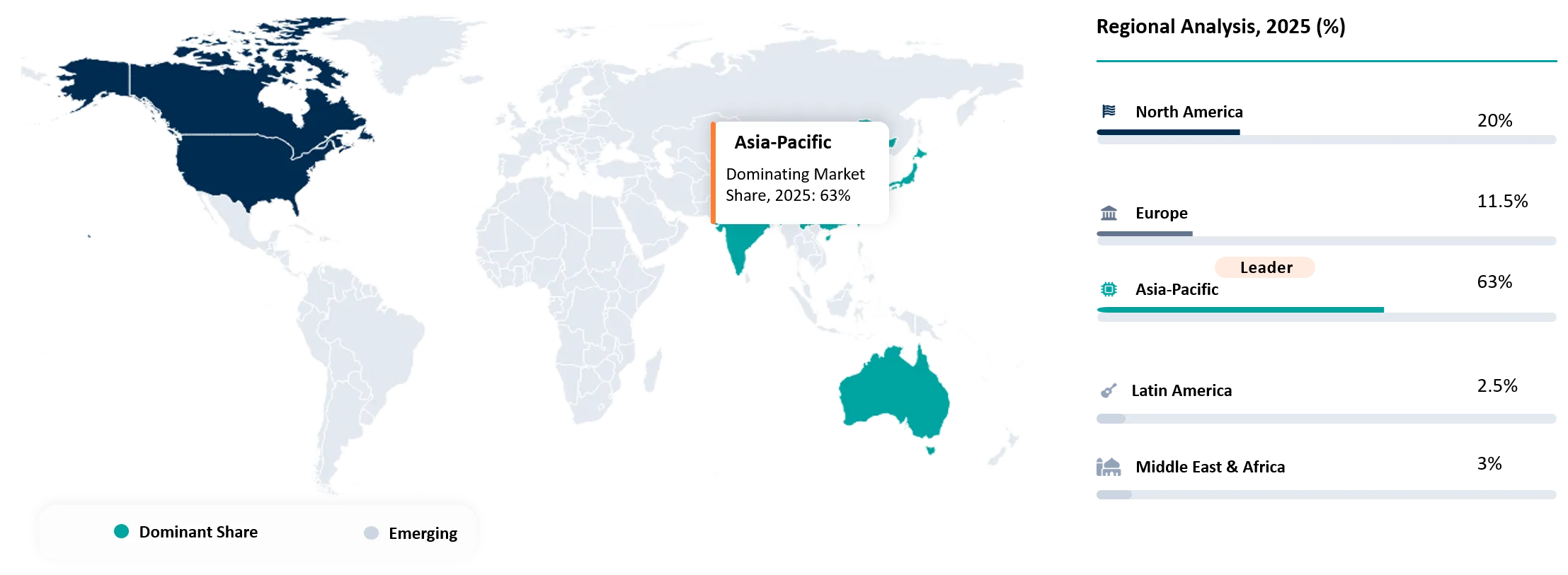
Rapid Semiconductor Manufacturing Expansion and Rising Water-Reclamation Investments Driving Asia-Pacific Dominance
The Asia-Pacific region dominates the semiconductor ultrapure water treatment market, with a 63% of market share in 2025, supported by the region’s strong concentration of semiconductor foundries, memory manufacturers, wafer fabrication facilities, and electronics manufacturing clusters across Taiwan, South Korea, China, and Japan. The rapid expansion of advanced logic, memory, AI, and high-performance computing semiconductor production is increasing the requirement for ultrapure water for wafer cleaning, rinsing, etching, lithography, and other fabrication processes. The presence of major semiconductor manufacturers and the continued development of new fabrication facilities are creating sustained demand for UPW generation, purification, monitoring, and wastewater-recycling systems.
India’s expanding semiconductor and advanced-manufacturing ecosystem is increasing demand for reliable ultrapure-water and water-recycling infrastructure. In November 2025, CN Tech Engineers Pvt. Ltd. (CN Water), an India-based high-purity water-system company, entered into a strategic MoU with Taiwan Pure Water Technology Co., Ltd. (Taipure), a Taiwan-based UPW technology company, to jointly bid for and execute ultrapure-water (UPW) and water-recycling projects across India’s semiconductor, green-energy, EV-battery, and precision-manufacturing sectors. Under the partnership, CN Water will lead project identification, tender participation, and on-site execution in India, while Taipure will provide strategic sourcing, design engineering, and commissioning support. The companies will initially target identified UPW and reclaim systems for semiconductor and EV manufacturing facilities. CN Water reports more than 35 years of experience, 2,200+ water systems installed and managed, and 150+ customer companies, while Taipure brings specialized semiconductor-grade UPW expertise.
China Semiconductor Ultrapure Water Treatment Market Trends
China holds a dominant position in the Asia-Pacific semiconductor ultrapure water treatment market due to its expanding semiconductor manufacturing base, increasing domestic wafer-fabrication capacity, and growing adoption of advanced water purification and recycling technologies. The country has a large concentration of foundries, integrated device manufacturers, and semiconductor production facilities, creating substantial and recurring demand for ultrapure water for wafer cleaning, rinsing, etching, lithography, and other fabrication processes. The continued development of domestic semiconductor capacity, particularly for mature and advanced process technologies, is increasing the need for reliable UPW generation and wastewater-treatment infrastructure.
China’s push for semiconductor self-reliance is accelerating the localization of critical manufacturing infrastructure, including advanced ultrapure-water treatment systems. In March 2025, GRINM Silicon Co., Ltd. (Youyan Silicon), a China-based semiconductor silicon-materials manufacturer, announced plans to acquire approximately 60% of High Frequency (Beijing) Technology Co., Ltd., a China-based ultrapure-water system supplier for the integrated-circuit industry, through a cash transaction, making High Frequency Technology its controlled subsidiary. High Frequency Technology provides ultrapure-water preparation, distribution, collection, treatment, reuse, and wastewater-treatment systems across the semiconductor manufacturing process and has developed technologies capable of supplying ppt-level ultrapure water, supporting the domestic substitution of foreign UPW technologies. The company is also recognized as a National-level “Little Giant” specialized and innovative enterprise.
Japan Semiconductor Ultrapure Water Treatment Market Outlook
Japan is a major country in the Asia-Pacific semiconductor ultrapure water treatment market owing to its established semiconductor manufacturing ecosystem, strong presence of wafer manufacturers, and renewed investment in advanced semiconductor production. The country hosts major semiconductor companies including Kioxia, Sony, Renesas, Micron, and SUMCO, while new investments in advanced logic and memory manufacturing are increasing the requirement for ultrapure water, wastewater treatment, and water-recycling infrastructure. Japan’s semiconductor ecosystem is also benefiting from government-backed efforts to strengthen domestic chip production, with advanced manufacturing projects creating additional demand for high-purity process water.
The rapid expansion of semiconductor and electronics manufacturing is increasing demand for flexible, high-purity water systems that can be deployed quickly. In October 2025, Kurita Water Industries Ltd., a Japan-based water-treatment technology company, announced that orders had begun for “e-WT,” an off-the-line ultrapure-water supply system developed for the electronics industry, including semiconductor manufacturing. The company states that the electronics industry's market size has doubled over the past 10 years and represents the largest share of industrial water usage, with demand expected to continue increasing. The e-WT system can reduce the EPC process by approximately 30% compared with conventional custom-made solutions by using prefabricated units that require no individual design, while producing ultrapure water from sources including industrial water and groundwater.
Rapid Semiconductor Fab Expansion and Increasing Water-Reuse Investments Driving North America’s Market Position
The North America region holds a significant position in the semiconductor ultrapure water treatment market, accounting for 20% of the market share in 2025, supported by the expansion of domestic semiconductor manufacturing, increasing investments in advanced logic and memory fabs, and the presence of major semiconductor manufacturers. The region is benefiting from the development of new fabrication facilities in the U.S., driven by demand for AI, high-performance computing, automotive, and advanced electronics. The combination of established semiconductor manufacturers, new foundry investments, and government-supported semiconductor localization is increasing the requirement for reliable ultrapure water generation, purification, recycling, and wastewater-treatment infrastructure.
The rapid expansion of semiconductor manufacturing in North America is increasing demand for advanced wastewater treatment, water recycling, and resource-recovery solutions. In December 2025, H2O Innovation Inc., a Canada-based water-treatment technology and services company, signed an exclusive teaming agreement with Fathom Water Corporation, a U.S.-based advanced water-treatment engineering and software company, to jointly pursue wastewater treatment and water-reuse projects for the North American semiconductor sector. Under the agreement, Fathom Water will lead business development, integrate complementary process technologies, and drive project execution, while H2O Innovation will provide membrane-based water and wastewater-treatment expertise, detailed engineering, U.S. fabrication, and ongoing services and consumables. H2O Innovation operates manufacturing facilities in the United States, including Minneapolis, where it fabricates skid-mounted treatment systems, piping spools, and panel assemblies.
U.S. Semiconductor Ultrapure Water Treatment Market Trends
The U.S. holds a dominant position in the North American semiconductor ultrapure water treatment market owing to its established semiconductor ecosystem, rapid expansion of domestic wafer-fabrication capacity, and increasing investments in advanced logic, memory, and AI semiconductor manufacturing. The presence of leading semiconductor manufacturers and foundries, together with government-backed efforts to strengthen domestic chip production, is accelerating the construction and expansion of fabrication facilities across Arizona, Texas, New York, and other semiconductor clusters. These developments are increasing the need for reliable ultrapure water systems for wafer cleaning, rinsing, etching, lithography, and other water-intensive fabrication processes.
The rapid expansion of advanced semiconductor manufacturing is increasing demand for highly specialized ultrapure-water systems and water-circularity solutions. In September 2025, Ecolab Inc., a U.S.-based water, hygiene, and sustainability solutions company, entered into a definitive agreement to acquire Ovivo’s Electronics business, a Canada-based ultrapure-water technology business, specializing in advanced UPW technologies for semiconductor manufacturing. Ecolab agreed to pay approximately USD 1.8 billion in cash, while Ovivo Electronics was expected to generate approximately USD 500 million in sales in 2025 and employed more than 900 people worldwide. The acquisition combines Ovivo Electronics’ ultrapure-water technologies with Ecolab’s water-treatment, digital, and global service capabilities to support advanced microchip manufacturing and water circularity.
Semiconductor Ultrapure Water Treatment Market Competitive Landscape
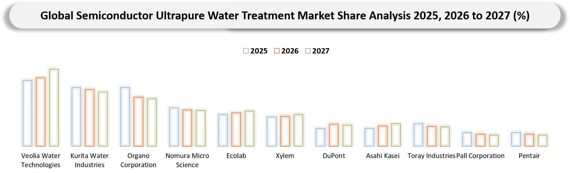
- The semiconductor ultrapure water treatment market is characterized by three key participant groups: integrated water-treatment providers, specialized ultrapure-water technology companies, and membrane, filtration, and water-reuse specialists. Veolia Water Technologies, Kurita Water Industries, Organo Corporation, Nomura Micro Science, and Ecolab focus on integrated UPW generation, wastewater treatment, water reclamation, and resource-recovery solutions for semiconductor manufacturing. Xylem, DuPont, Asahi Kasei, Toray Industries, and Pall Corporation provide advanced membrane, filtration, ion-exchange, separation, and purification technologies, while Pentair and Aquatech International offer water-treatment, reuse, and resource-recovery solutions. This creates a highly technology-driven and ecosystem-oriented landscape where UPW purity, contamination control, system reliability, water recovery, process integration, and customer-specific solutions define competitiveness.
- Key players include Veolia Water Technologies (France), Kurita Water Industries (Japan), Organo Corporation (Japan), Nomura Micro Science (Japan), Ecolab (U.S.), Xylem (United States), DuPont (U.S.), Asahi Kasei (Japan), Toray Industries (Japan), Pall Corporation (U.S.), Pentair (U.S.), and Aquatech International (U.S.).
Key Developments
- June 2025: Aquatech, a U.S.-based industrial water and process-technology company, acquired Century Water, a Singapore-based water-treatment company specializing in ultrapure process water and wastewater recycling for the semiconductor, pharmaceutical, and advanced-manufacturing sectors.
- May 2026: Industrie De Nora S.p.A., an Italy-based electrochemistry and water-treatment technology company, signed an agreement to acquire 100% of BW Water Pte. Ltd., a Singapore-based engineering, procurement and fabrication (EPF) water-treatment company specializing in industrial and semiconductor wastewater, ultrapure water, desalination, and integrated water solutions.
- June 2026: Membrane Group India, an India-based process-water and wastewater-treatment company, formed a joint venture with Kurita Water Industries, a Japan-based water-treatment technology company, to establish Kurita Membrane India Pvt. Ltd. for India’s semiconductor and electronics manufacturing sector.
- June 2026: Coway Entech Co., Ltd., a South Korea-based industrial water-treatment company and wholly owned subsidiary of Coway, established COWAY ENTECH USA, INC. in Indiana, U.S., marking its first overseas subsidiary and creating a local base for industrial water-treatment services in North America.
- August 2026: Gradiant, a U.S.-based advanced water and wastewater-treatment technology company, expanded its U.S. operations to support the rapidly growing water requirements of AI infrastructure, semiconductor manufacturing, and data centers.
Key Procurement Priorities and Buyer Evaluation Criteria
- Organizations investing in the Semiconductor Ultrapure Water Treatment Market increasingly select suppliers based on their ability to deliver high-purity, reliable, and continuous UPW systems capable of meeting stringent semiconductor manufacturing requirements. Buyers prioritize suppliers with proven capabilities in UPW generation, purification, polishing, filtration, distribution, and wastewater treatment while ensuring stable water quality across high-volume fabrication operations.
- The procurement decision-making process is increasingly influenced by the expansion of advanced semiconductor nodes, AI and high-performance computing chips, 3 nm and 2 nm manufacturing, and increasing wafer-fabrication capacity, which require tighter contamination control and highly consistent water quality. Buyers therefore evaluate suppliers based on their ability to support increasingly demanding semiconductor processes while maintaining uninterrupted UPW availability and process stability.
- Buyers consider factors such as UPW resistivity, total organic carbon (TOC), particle and microbial control, trace-metal removal, system reliability, water-recovery rates, and continuous quality monitoring when selecting their water-treatment technology partners. The ability to maintain consistent ultrapure-water quality throughout wafer cleaning, rinsing, lithography, etching, deposition, and chemical mechanical planarization processes is a key procurement consideration.
Why Choose DataM?
- Technological Innovations: Explores advancements in semiconductor ultrapure water treatment, including advanced membrane filtration, reverse osmosis, ion exchange, electrodeionization, ultraviolet oxidation, ultrafiltration, and point-of-use polishing technologies, enabling fabs to achieve stringent purity requirements while improving water recovery and treatment efficiency.
- System Performance & Market Positioning: Evaluates how different players deliver UPW solutions based on resistivity, TOC control, particle removal, trace-metal reduction, microbial control, system reliability, water-recovery rates, and energy efficiency, highlighting how leading suppliers differentiate through integrated treatment systems and semiconductor-specific capabilities.
- Real-World Evidence: Highlights the deployment of ultrapure water treatment and reclamation systems across semiconductor fabs, wafer fabrication facilities, and advanced-node manufacturing sites, demonstrating their role in wafer cleaning, rinsing, etching, lithography, deposition, and chemical mechanical planarization while supporting yield, contamination control, and water conservation.
- Market Updates & Industry Changes: Tracks key developments such as new semiconductor fab construction, advanced-node capacity expansion, UPW system installations, water-reclamation projects, recycling initiatives, and technology investments across Asia-Pacific, North America, and Europe, supporting the transition toward more water-efficient semiconductor manufacturing ecosystems.
- Competitive Strategies: Analyzes how leading companies expand through technology development, fab-scale system deployment, strategic partnerships, acquisitions, regional expansion, and integrated water-treatment offerings, while strengthening capabilities in UPW generation, wastewater treatment, water reclamation, and resource recovery.
- Pricing & Market Access: Evaluates pricing differences based on treatment capacity, required purity levels, process complexity, technology configuration, automation, water-recovery requirements, and system scale, while examining market access through direct contracts with semiconductor manufacturers, engineering companies, foundries, and fab developers.
- Market Entry & Expansion: Identifies growth opportunities driven by AI semiconductor production, advanced logic and memory manufacturing, 3 nm and 2 nm process development, semiconductor localization, and new fab construction, while outlining strategies such as localized service networks, water-reuse integration, technology differentiation, and long-term partnerships with semiconductor manufacturers.
Target Audience 2026
- Semiconductor Manufacturers and Foundries
- Water Treatment and UPW Technology Providers
- Semiconductor Fab Facility Engineers
- Process and Manufacturing Engineers
- Semiconductor Equipment and Materials Suppliers
- Environmental, Sustainability, and Water-Management Teams
- Investors, Consultants, and Industry Analysts