Semiconductor Materials Market Size and Overview
The global semiconductor materials market was valued at approximately US$ 71.0 billion in 2025 and is projected to reach about US$ 115.6 billion by 2035, expanding at an estimated CAGR of approximately 5.0% during 2026-2035. Growth is supported by AI accelerators, HBM, advanced logic, 3D NAND, power semiconductors, EUV adoption and increasingly material-intensive advanced packaging.
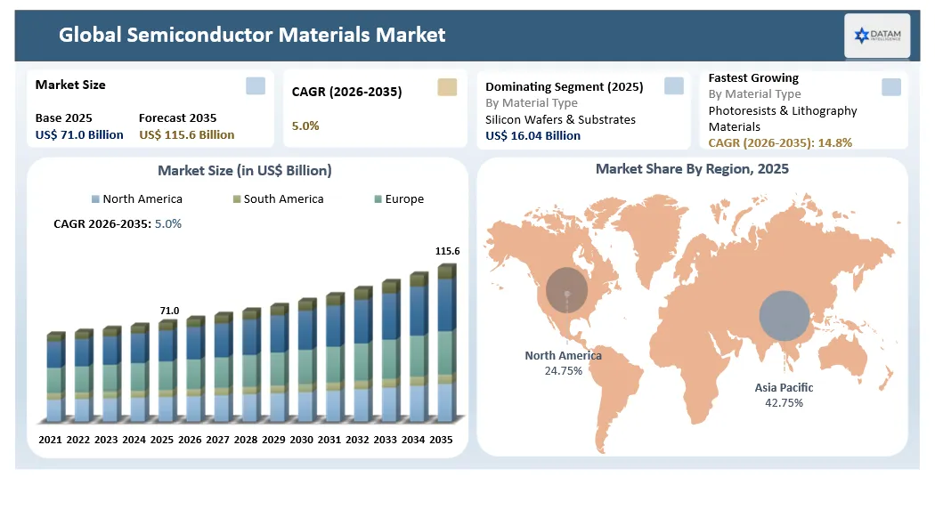
Asia-Pacific remains the dominant production and materials-consumption center due to Taiwan, South Korea, China and Japan. North America is gaining incremental share through leading-edge fab and packaging investment, while Europe is supported by automotive, power semiconductor and strategic manufacturing programs. Qualification depth, purity, defectivity, supply continuity and local technical support are increasingly decisive sourcing criteria.
| Metric | Semiconductor Materials Market Insight |
| 2025 Market Size | ~US$ 71.0 billion |
| 2035 Market Size | ~US$ 115.6 billion |
| 2026-2035 CAGR | ~5.0% |
| Largest Region | Asia-Pacific (~42.75% estimated share in 2025) |
| High-Growth Material Areas | EUV photoresists, CMP consumables, ALD/CVD precursors, HBM/advanced packaging materials |
| Demand Anchor | AI/HPC, HBM, advanced logic, 3D NAND and fab localization |
| Key Procurement Criteria | Purity, defectivity, qualification history, continuity of supply, local technical support |
| Strategic Risk | Geographic concentration, long qualification cycles, feedstock constraints and environmental regulation |
Semiconductor Materials Market Key Takeaways
- Asia-Pacific accounts for an estimated 78.5% of 2025 semiconductor materials revenue because the region contains the largest concentration of logic, memory, foundry and packaging capacity.
- AI accelerators and HBM increase demand for advanced wafers, deposition materials, photoresists, CMP consumables, materiales and packaging materials across multiple process steps.
- EUV and gate-all-around transitions raise material purity and defect-control requirements, strengthening the value of qualified high-performance formulations.
- Advanced packaging shifts material value toward dielectric films, underfills, mold compounds, temporary bonding materials, redistribution-layer chemistry and thermal-interface solutions.
- Supply localization in the United States, Japan, Europe, India and Southeast Asia is creating opportunities for regional purification, blending, reclaim and technical-service capacity.
- Silicon wafers remain one of the largest material categories, while photoresists, CMP, deposition materials and packaging materials offer above-market growth in leading-edge applications.
- Supplier qualification can take months or years, creating sticky customer relationships but also raising switching costs and supply-concentration risk.
- The market ecosystem is tightly coupled across EDA, semiconductor fabrication, materials purification and delivery equipment, material purification processes, materiales, consumables, OSATs, material suppliers and end-device designers.
Semiconductor Materials Industry Trends and Strategic Insights
- Semiconductor manufacturing is moving toward EUV lithography, gate-all-around transistors, backside power delivery, HBM, higher-layer 3D NAND and heterogeneous integration. These architectures increase the number and precision of deposition, etch, clean, CMP, lithography and packaging steps, raising the value of qualified semiconductor materials per wafer.
- Materials suppliers are investing in tighter defect control, atomic-level purity, advanced filtration and formulation consistency. The commercial advantage increasingly comes from co-development with equipment makers and fabs, where a material can improve yield, enable a smaller feature size or reduce process variability.
- Advanced packaging is expanding the addressable materials pool beyond front-end wafer fabrication. Hybrid bonding, redistribution layers, chiplets and 2.5D/3D integration are increasing demand for dielectric films, temporary bonding materials, underfills, mold compounds, plating chemistry and thermal-interface materials.
- Cyclicality remains important. Silicon wafers and several high-volume chemicals are sensitive to fab utilization, while differentiated resists, CMP slurries, deposition precursors and packaging formulations can sustain stronger pricing because qualification and switching costs are high.
- Supply-chain resilience is encouraging localized purification, blending, warehousing and technical-service capacity near new fab clusters in the United States, Japan, Europe, India and Southeast Asia. However, Northeast Asia remains the largest production and consumption base.
- Policy support is reshaping supplier footprints. Semiconductor incentive programs increasingly encourage domestic ecosystems for wafers, photoresists, chemicals, gases, substrates and packaging materials, while environmental regulation is accelerating solvent recovery, chemical substitution and lower-impact formulations.
Semiconductor Materials Market Scope
| Metrics | Assessment |
| High Regulation Impact | High-purity chemical handling, PFAS scrutiny, emissions controls, chemical registration and worker-safety requirements influence materials portfolios. |
| High Investment Activity | New fabs, HBM lines and advanced packaging capacity require local materials qualification, purification, warehousing and delivery infrastructure. |
| Supply Chain Disruption | Photoresist inputs, silicon wafers, rare metals, high-purity chemicals and specialized polymers can have concentrated supply bases. |
| Pricing Volatility | Energy, fluorochemicals, metals, solvents and silicon feedstock affect cost while long qualification cycles constrain substitution. |
| Procurement Pressure | Fabs increasingly require dual sourcing, local inventory, traceability, low defectivity and rapid technical response. |
| New Technology Adoption | EUV, GAA, backside power, HBM, hybrid bonding and chiplets create new formulation and purity requirements. |
| Regional Expansion Opportunity | United States, Japan, Europe, India and Southeast Asia offer localization opportunities alongside core Northeast Asian capacity. |
| Government Policy Support | Semiconductor incentive programs increasingly encourage domestic supplier ecosystems and materials security. |
| Pricing Intelligence | Contract terms depend on qualification status, purity, volume, local service, raw-material pass-through and strategic scarcity. |
Why does this report matter in 2026?
In 2026, AI-related semiconductor capacity, HBM, advanced logic and heterogeneous packaging are expanding while governments are funding new fabs across the United States, Japan, Europe and Asia. Each new fab requires a qualified ecosystem for wafers, resists, wet chemicals, CMP materials, deposition precursors, electronic gases and packaging materials, creating multi-year opportunities for suppliers that qualify early.
The report matters because semiconductor-material competitiveness is determined by more than production capacity. Purity, defectivity, lot-to-lot consistency, qualification history, local technical support, change-control discipline and continuity of supply directly influence fab yield and customer switching costs.
Semiconductor Materials Market White Space & Investment Opportunities
- White-space opportunities include regional purification and blending near new fab clusters, EUV and high-NA patterning materials, advanced-node wet chemicals, selective deposition precursors, next-generation CMP slurries, engineered substrates, wafer reclaim and recycling, PFAS-reduced formulations and advanced packaging polymers.
- EUV and high-NA lithography create opportunities in chemically amplified resists, metal-oxide resists, underlayers and contamination-control materials.
- HBM, chiplets and hybrid bonding expand demand for temporary bonding, dielectric films, underfills, plating chemistry, mold compounds and high-performance thermal-interface materials.
- Lower-carbon and circular materials are gaining importance through solvent recovery, wafer reclaim, chemical recycling, renewable-power use and product-level carbon accounting.
- Localized materials capacity in the United States, Japan, Europe, India and Southeast Asia can reduce geopolitical and logistics risk for fabs that require qualified regional supply.
- AI-enabled quality control, advanced filtration, digital traceability and in-line metrology create opportunities to reduce contamination, lot variation and yield loss.
Semiconductor Materials Future Market Transformation
By 2035, the market will be more tightly integrated with device and equipment roadmaps. Leading suppliers will increasingly co-develop materials for EUV, GAA, backside power, selective deposition, HBM, hybrid bonding and advanced substrates rather than sell generic chemistries. Quality data, defectivity and sustainability metrics will become as important as nominal chemical specifications.
Business models will continue to combine global scale with local service. Long-term supply agreements, customer-dedicated purification, local technical centers, inventory buffers and joint development programs will become more common where qualification cycles are long and supply interruption carries high yield risk.
Semiconductor Materials Market Buyer Decision-Making Criteria
Buyers prioritize qualified electrical and process performance, purity, trace-metal limits, particle counts, defectivity, lot consistency, shelf life, packaging integrity, local inventory, change notification, supplier financial strength and rapid technical response. For advanced-node materials, yield impact often outweighs unit price.
Semiconductor Materials Market Economic & Investment Analysis
Economics differ sharply by category. Silicon wafers and basic process chemicals are more exposed to utilization cycles and energy or feedstock costs, while leading-edge resists, CMP, deposition materials and packaging formulations can earn higher margins through intellectual property, qualification depth and technical service.
Investment is shifting toward advanced-node formulations, 300 mm and engineered substrates, local purification and blending, EUV materials, HBM and packaging materials, contamination-control infrastructure and circular-material capabilities rather than undifferentiated commodity capacity.
Semiconductor Materials Investment Trends in the Market
- Foundries, memory manufacturers and OSATs are expanding local supplier qualification programs alongside fab and advanced-packaging capacity.
- Materials suppliers are increasing capacity for 300 mm wafers, EUV resists, CMP slurries, deposition precursors, high-purity chemicals and advanced packaging formulations aligned with AI and HBM roadmaps.
- Equipment and contamination-control vendors are investing in filtration, chemical delivery, dispense, metrology and process-control systems that protect material purity from supplier to point of use.
- Substrate and packaging-material suppliers are developing SOI, silicon carbide, glass-core, low-loss dielectric and high-performance polymer platforms for heterogeneous integration.
- Partnerships increasingly link fabs, OSATs, equipment companies and materials suppliers to qualify complete process stacks before high-volume manufacturing.
Strategic Indicators for Semiconductor Materials Market
High Regulation Impact
Export controls, semiconductor incentives, chemical regulations, worker-safety rules and supply-chain security policies influence where advanced semiconductor materials can be produced, qualified and sold.
High Investment Activity
Semiconductor materials are attracting capital across wafers, EUV resists, CMP, deposition materials, packaging polymers, purification, reclaim and local technical-service infrastructure.
Supply Chain Disruption
Concentration in silicon wafers, photoresist inputs, high-purity chemicals, specialty metals and selected precursor chemistries can create allocation risk and delay fab ramps when alternate suppliers are not qualified.
Pricing Volatility
Pricing varies with purity, formulation complexity, defectivity, qualification status, feedstock costs, volume commitments and local service requirements. Leading-edge and supply-constrained materials command premiums over mature-node commodity grades.
Procurement Pressure
Fab buyers face pressure to secure dual sources, maintain strategic inventory, qualify local alternatives and improve traceability without introducing process variation or yield risk.
New Technology Adoption
Hybrid bonding, through-glass vias, next-generation substrates, backside power delivery, wafer-to-wafer stacking and thermal-aware materials design are changing integration strategies.
Regional Expansion Opportunity
Asia-Pacific remains the manufacturing center, while North America, Europe and Japan are expanding domestic fab and materials ecosystems. India and Southeast Asia offer emerging opportunities in packaging, chemicals and regional supply-chain support.
Government Policy Support
CHIPS-style incentives and national semiconductor strategies increasingly include local materials suppliers, R&D centers, pilot lines, chemical infrastructure and advanced-packaging ecosystems.
Pricing Intelligence
Pricing intelligence requires category-level analysis because wafer contracts, photoresists, CMP, wet chemicals, deposition precursors and packaging materials have different cost drivers and qualification economics.
Disruption Analysis of Semiconductor Materials Market
The market is being disrupted by EUV and high-NA lithography, selective deposition, GAA transistors, HBM, chiplets, hybrid bonding, engineered substrates and stricter environmental requirements. These shifts move value toward suppliers that can deliver atomic-scale purity, defect control, co-development and regional supply resilience.
Semiconductor Materials Market BCG Matrix: Company Evaluation
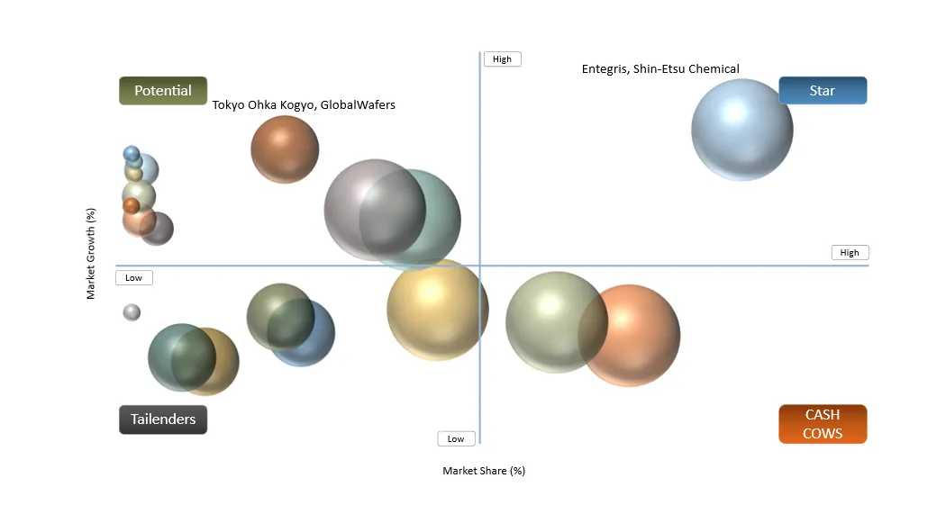
STAR
Entegris, Shin-Etsu Chemical, SUMCO and Merck KGaA / EMD Electronics occupy strong strategic positions because they combine scale, deep qualification histories, broad semiconductor exposure and technology roadmaps aligned with leading-edge fabs.
POTENTIAL
Tokyo Ohka Kogyo, GlobalWafers, Soitec, DuPont, Resonac and Fujifilm Electronic Materials represent high-potential or category-leading specialists across photoresists, engineered substrates, CMP, packaging materials and advanced process chemistries.
Semiconductor Materials Market Dynamics
Driver Impact Analysis
| Driver | 2026-2028 Impact | 2029-2032 Impact | 2033-2035 Impact | Strategic Meaning |
| AI, HBM & advanced-node capacity | High | Very High | Very High | Raises consumption of wafers, resists, CMP, deposition and packaging materials |
| Fab localization & capacity expansion | High | High | Medium-High | Creates regional qualification and local-supply opportunities |
| Advanced packaging / chiplets | High | Very High | Very High | Expands polymer, bonding, RDL, underfill, mold and thermal-material demand |
| EUV, GAA & process complexity | High | Very High | Very High | Increases purity, defect-control and materials-intensity requirements |
Driver: AI, HBM, Advanced Logic and Fab Localization Increasing Semiconductor Materials Intensity
AI accelerators, HBM and advanced logic require more process steps, tighter defect control and increasingly specialized materials. New fabs also need localized, qualified supplier networks, raising demand for wafers, resists, CMP, wet chemicals, deposition materials, electronic gases and advanced packaging materials.
Restraint Impact Analysis
| Restraint | 2026-2028 Impact | 2029-2032 Impact | 2033-2035 Impact | Strategic Meaning |
| Semiconductor cyclicality | High | Medium | Medium | Fab utilization swings affect materials volumes and pricing |
| Long qualification cycles | High | High | High | Slows new supplier penetration but protects incumbents |
| Geographic / feedstock concentration | High | High | Medium-High | Raises inventory and dual-sourcing requirements |
| Environmental & safety compliance | Medium-High | High | High | Drives reformulation, abatement, recycling and process changes |
Restraint: Semiconductor Cyclicality, Qualification Barriers and Supply Concentration
Fab utilization swings can reduce demand for high-volume materials, while long qualification cycles make it difficult for customers to switch suppliers quickly. Concentrated production of silicon wafers, photoresist inputs, specialty metals and selected chemistries also raises geopolitical and continuity risk.
Semiconductor Materials Market Segment Analysis
The global Semiconductor Materials market is segmented based on Material Type, Process / Application, Purity / Material Grade, Form / Delivery Mode, Application, End Use Industry, Supplier / Customer Model, Substrate / Material Platform and region.
By Material Type
Silicon Wafers & Substrates Will Continue to Lead Market Value
Silicon wafers and engineered substrates remain one of the largest value pools because every semiconductor starts with a highly controlled substrate. Growth is supported by 300 mm advanced logic and memory, silicon-on-insulator, silicon carbide and other engineered substrates, even as mature-node wafer demand remains more cyclical.
By Process / Application
Lithography, Deposition and CMP Materials Will Record Above-Market Growth
EUV and advanced patterning increase demand for high-performance resists and underlayers, while GAA and 3D architectures require more deposition and CMP steps. These categories benefit from high qualification barriers and direct influence on yield, making them strategic growth areas.
By Purity / Material Grade
Electronic / Semiconductor Grade Will Remain the Largest Product Segment
Electronic and ultra-high-purity grades account for most market value because semiconductor fabs impose strict limits on particles, metals, moisture and organic contamination. Advanced-node materials require even tighter specifications and more intensive analytical control.
By Form / Delivery Mode
Bulk and Fab-Integrated Delivery Will Gain Share in High-Volume Fabs
High-volume fabs increasingly use bulk chemical delivery, automated dispense and closed-loop contamination-control systems, while packaged materials remain essential for low-volume, high-value and specialty formulations. Delivery architecture becomes part of the qualification envelope for critical materials.
By Application
Logic, Memory and Advanced Packaging Will Lead Growth
AI/HPC logic, HBM, 3D NAND and advanced packaging are the strongest value-growth applications because they combine high wafer starts with greater process complexity and materials intensity.
By End Use Industry
AI, Data Center and High-Performance Computing Will Drive Premium Demand
AI servers, accelerators, networking and data-center infrastructure are increasing demand for leading-edge logic, HBM and advanced packaging. Automotive, industrial and communications applications provide additional growth through power semiconductors, sensors and connectivity devices.
Semiconductor Materials Market Geographical Penetration
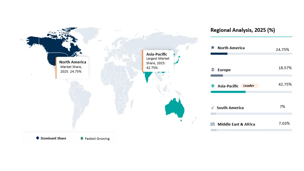
Estimated share of global semiconductor materials revenue across the five report regions. Shares are modeled from fab capacity, semiconductor production concentration and published electronic specialty-material benchmarks and sum to 100%.
| Region | 2025 Estimated Market Share | Market Position / Demand Base |
| Asia-Pacific | 42.75% | Largest semiconductor manufacturing base; Taiwan, South Korea, China and Japan dominate materials consumption |
| North America | 24.75% | Leading-edge logic, memory, AI packaging and U.S. fab localization |
| Europe | 18.57% | Automotive, power semiconductor, specialty logic and strategic fab programs |
| Middle East & Africa | 7.03% | Emerging semiconductor investment, packaging and electronics manufacturing |
| South America | 7.0% | Smaller fabrication base; demand centered on electronics assembly and specialty semiconductor operations |
U.S. Semiconductor Materials Market Landscape
The U.S. is a major market for advanced semiconductor design and is rapidly expanding domestic fabrication and packaging. New leading-edge logic, memory and foundry investments create opportunities for local wafer, chemical, CMP, lithography, deposition and contamination-control suppliers.
China Semiconductor Materials Market Trends
China remains a major semiconductor manufacturing and electronics market and continues to expand domestic materials capability. Localization is strongest in mature-node chemicals, wafers, targets and selected photoresists, while export controls and technology restrictions shape access to leading-edge inputs.
Japan Semiconductor Materials Market Outlook
Japan is one of the world’s most important semiconductor-materials supply bases, with global leadership in silicon wafers, photoresists, high-purity chemicals, substrates and packaging materials. Public-private investment in new fabs strengthens domestic demand and qualification activity.
Germany Semiconductor Materials Market Outlook
Germany and wider Europe combine automotive electronics, power semiconductors, specialty logic, sensors and advanced research. Growth opportunities center on materials for SiC/GaN, automotive chips, new foundry capacity and European supply-chain resilience.
Middle East Semiconductor Materials Market Outlook
The Middle East remains an emerging semiconductor materials market. Near-term demand is tied to electronics manufacturing, data centers and selected packaging or specialty semiconductor projects, while longer-term opportunities depend on regional fab and advanced-manufacturing investment.
Semiconductor Materials Market Competitive Landscape
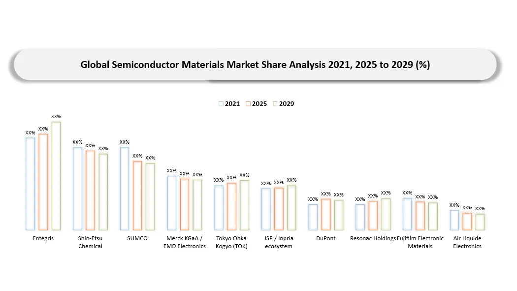
- Competition is structured around qualification depth, material purity, defectivity, intellectual property, scale, customer co-development and local technical support. The market includes broad materials platforms as well as highly specialized leaders in wafers, resists, CMP, chemicals, targets and packaging materials.
- Entegris, Shin-Etsu Chemical, SUMCO, Merck KGaA / EMD Electronics and Tokyo Ohka Kogyo are major public companies with direct exposure to semiconductor materials. GlobalWafers, Soitec, DuPont, Resonac, Fujifilm, JX Advanced Metals and other specialists strengthen category-specific competition.
- Competition increasingly extends beyond product chemistry into contamination control, digital quality data, local inventory, reclaim, sustainability and rapid co-development with equipment and device makers.
- Market share is sticky where materials are deeply qualified, but technology transitions can shift value quickly toward suppliers that solve new patterning, deposition, planarization, substrate or packaging challenges.
- Differentiation therefore depends on yield impact, purity, defectivity, process-window performance, supply continuity and the ability to support customers through rapid node and packaging transitions.
Market Ecosystem Table
| Value Chain Sector | Representative Companies | Role in Semiconductor Materials Market |
| Raw Materials & Feedstocks | Hemlock Semiconductor, Wacker Chemie, BASF, Solvay, metal and fluorochemical suppliers | Polysilicon, solvents, acids, fluorochemicals, metals and specialty feedstocks |
| Silicon Wafers & Substrates | Shin-Etsu Handotai, SUMCO, GlobalWafers, Soitec, SK Siltron | 300 mm/200 mm silicon, SOI and engineered substrates |
| Photoresists & Lithography | Tokyo Ohka Kogyo, JSR, Shin-Etsu Chemical, DuPont, Fujifilm | EUV/ArF/KrF photoresists, developers, anti-reflective and ancillary materials |
| Process Chemicals & CMP | Entegris, Merck/EMD Electronics, Fujifilm, Resonac, DuPont, CMC Materials legacy portfolio | Ultra-high-purity chemicals, slurries, pads and surface-treatment materials |
| Electronic Gases & Precursors | Air Liquide, Linde, Air Products, Merck/EMD Electronics, Resonac | Etch, deposition, cleaning and doping gases/precursors |
| Targets & Thin-Film Materials | JX Advanced Metals, Tosoh, Materion, Umicore and specialty target suppliers | Sputtering targets, high-purity metals and deposition materials |
| Advanced Packaging Materials | Resonac, Henkel, Namics, Ajinomoto, DuPont, Shin-Etsu Chemical | Underfills, dielectric films, mold compounds, bonding and thermal materials |
| Delivery / Contamination Control | Entegris, Ichor Systems, MKS Instruments and specialist integrators | Filters, containers, fluid handling, chemical delivery and contamination control |
| Fabs / IDMs / Foundries | TSMC, Samsung, SK hynix, Micron, Intel, GlobalFoundries | Primary material qualification authorities and high-volume consumers |
| OSAT / Advanced Packaging | ASE, Amkor, JCET and foundry packaging operations | Packaging-material demand and advanced heterogeneous integration |
| Standards / Regulators | SEMI, EPA, ECHA, OSHA and national chemical regulators | Material standards, safety, emissions, chemical registration and sustainability requirements |
Public Company Q1-Q2 2026 Performance Comparison
| Public Company | Reporting Period | Q1-Q2 2026 Performance | Growth Indicator | Factors Driving Semiconductor Materials Exposure |
| Entegris | Q1-Q2 2026 | Q1 2026 results and Q2 2026 reporting emphasized semiconductor demand and advanced materials/process solutions; Q2 guidance was US$815-845M before the release. | AI, leading-edge logic and memory support content-per-wafer growth. | CMP, liquid filtration, specialty chemicals, advanced deposition materials, containers and contamination control. |
| Shin-Etsu Chemical | Apr-Jun 2026 / Q1 FY2027 | Q1 financial data was released July 24, 2026. Semiconductor silicon remained a core Electronics Materials business with 300 mm wafer demand supported by advanced applications. | Leading-edge wafer demand and technology migration support premium substrate mix. | Global silicon-wafer leadership plus photoresists, photomask blanks, quartz and encapsulation materials. |
| SUMCO | H1 2026 reporting window | 2026 results reflect a gradual semiconductor-wafer recovery against a still-disciplined utilization environment, with 300 mm leading-edge demand structurally stronger than mature-node categories. | AI, advanced logic and memory recovery support 300 mm wafer demand. | High-purity 300 mm and 200 mm silicon wafers for leading semiconductor manufacturers. |
| Merck KGaA / EMD Electronics | Q1-Q2 2026 | Electronics benefited from stronger semiconductor materials demand in 2026, with semiconductor solutions tied to AI and advanced-node investment. | Semiconductor Solutions growth supported by advanced-node and AI infrastructure demand. | Deposition materials, specialty gases, patterning materials and integrated semiconductor solutions. |
| Tokyo Ohka Kogyo (TOK) | Q1-Q2 2026 | Q1 2026 results were released May 11 and Q2 results on August 6, with the company focused on high-end photoresists and advanced packaging materials. | EUV/ArF photoresists and high-end packaging materials remain major strategic growth areas. | Leading photoresists, high-purity chemicals and semiconductor packaging materials. |
Key Companies
- Entegris
- Shin-Etsu Chemical
- SUMCO
- Merck KGaA / EMD Electronics
- Tokyo Ohka Kogyo (TOK)
- JSR / Inpria ecosystem
- DuPont
- Resonac Holdings
- Fujifilm Electronic Materials
- Air Liquide Electronics
- Linde Electronics
- Air Products Electronics
- BASF Electronic Materials
- Mitsubishi Chemical Group
- AGC
Company Profiles
Entegris
Entegris is a leading supplier of advanced materials and process solutions for semiconductor manufacturing. Its portfolio spans CMP materials, specialty chemicals, advanced deposition materials, filters, fluid handling, wafer shippers and contamination-control systems, giving it broad exposure to leading-edge logic, memory and advanced packaging.
Shin-Etsu Chemical
Shin-Etsu Chemical is one of the world’s largest semiconductor silicon-wafer suppliers and also supplies photoresists, photomask blanks, synthetic quartz, encapsulation materials and other electronics materials. Its scale and long qualification history make it a critical supplier to advanced logic and memory fabs.
SUMCO
SUMCO is a major global producer of 300 mm and 200 mm silicon wafers. Its competitive position is tied to leading-edge wafer quality, long-term customer relationships and the pace of memory and logic utilization recovery.
Merck KGaA / EMD Electronics
Merck KGaA / EMD Electronics supplies semiconductor solutions across deposition materials, specialty gases, patterning materials, dielectric and planarization-related chemistries. Its portfolio is positioned around advanced-node logic, memory and AI-driven semiconductor investment.
Tokyo Ohka Kogyo (TOK)
Tokyo Ohka Kogyo (TOK) is a major supplier of photoresists and high-purity chemicals used in semiconductor lithography, with strategic emphasis on EUV, ArF and advanced packaging materials. Its close collaboration with leading fabs and equipment makers supports high qualification barriers.
JSR / Inpria ecosystem
JSR and the Inpria ecosystem are important in advanced lithography materials, including leading-edge photoresists and metal-oxide resist technology. Their value is concentrated in patterning innovation and co-development for advanced nodes.
DuPont
DuPont supplies a broad range of semiconductor and advanced packaging materials, including dielectric, metallization, lithography-adjacent and packaging solutions. Its portfolio benefits from rising chiplet, redistribution-layer and heterogeneous-integration demand.
Fujifilm Electronic Materials
Fujifilm Electronic Materials supplies high-purity process chemicals, CMP materials, photoresists and other semiconductor materials. Its global manufacturing footprint and technical-service capabilities support both leading-edge and mature-node customers.
BASF Electronic Materials
BASF Electronic Materials supplies high-purity process chemicals and specialty formulations used across semiconductor fabrication. The business is positioned around stringent purity requirements, localized supply and process-chemistry expertise.
Additional Company Coverage
Additional profiles and benchmarking include Resonac Holdings, GlobalWafers, Soitec, JX Advanced Metals, Air Liquide Electronics, Linde Electronics, Air Products Electronics, Mitsubishi Chemical Group and AGC across wafers, engineered substrates, targets, electronic gases, process chemicals and advanced packaging materials.
Semiconductor Materials Market Major Pain Points
- Long qualification cycles can delay new supplier entry and make capacity expansion risky if customer ramps are slower than expected.
- Particle, metal and organic contamination at trace levels can reduce yield, forcing suppliers to invest heavily in purification, filtration, packaging and analytical control.
- Supply concentration in wafers, photoresist inputs, specialty metals and selected precursor chemistries increases geopolitical and logistics risk.
- Semiconductor cyclicality can leave high-volume wafer and chemical assets underutilized, compressing margins during memory and mature-node downturns.
- Environmental rules covering solvents, fluorinated chemistries, PFAS, hazardous chemicals, emissions and waste treatment can require costly reformulation and process changes.
- Rapid transitions to EUV, GAA, HBM and advanced packaging can shorten the commercial life of older material formulations and require repeated qualification investment.
- New fabs demand local inventory and technical support before volume ramps, creating working-capital and staffing requirements for suppliers entering new regions.
- Raw-material purity, energy, logistics, container availability and specialty feedstock costs can create pricing volatility across material categories.
Semiconductor Materials Market Recent Developments
- August 2026: Tokyo Ohka Kogyo announced its second-quarter 2026 financial results, with strategic focus continuing on high-end photoresists and semiconductor packaging materials.
- August 2026: Entegris reported second-quarter 2026 results after guiding to US$815-845 million of quarterly sales, with semiconductor demand and advanced materials remaining the core earnings drivers.
- July 2026: Shin-Etsu Chemical released first-quarter financial data for the period ended June 30, 2026, with semiconductor silicon remaining a core Electronics Materials business.
- 2026: SUMCO continued managing silicon-wafer utilization and investment against a gradual demand recovery, with advanced 300 mm applications structurally stronger than mature-node categories.
- 2026: Merck KGaA / EMD Electronics highlighted stronger semiconductor materials demand as AI, advanced-node logic and memory investment supported its Electronics business.
- 2026: Materials suppliers accelerated localization, reclaim, lower-impact formulations and technical-service expansion near new fab clusters in the United States, Japan, Europe and Asia.
Analyst View / Opinion on Semiconductor Materials Market
- Semiconductor materials form the foundation of every wafer-fabrication and advanced-packaging process. Strategic importance is increasing because AI, HBM and advanced logic require more process steps, tighter defect control and more specialized chemistries, while fab localization encourages geographically resilient supply networks.
- Near-term leadership will be determined by qualification depth, purity, defectivity, process-window performance, customer co-development and continuity of supply. Suppliers that can scale new formulations without introducing lot variation will capture disproportionate value.
- Advanced logic, AI accelerators, HBM and 3D NAND will remain the largest near-term demand engines, while advanced packaging and power semiconductors broaden opportunities across front-end and back-end materials.
- EUV resists, selective deposition materials, next-generation CMP, engineered substrates, packaging polymers and high-performance thermal materials should outgrow the broader market as device architectures become more complex.
- Global-scale suppliers retain advantages in qualification history and customer reach, while specialized materials companies can win through category leadership, faster innovation and close technical collaboration with fabs and equipment makers.
- Contamination-control, delivery, reclaim, metrology and process-control suppliers can capture additional value as fabs tighten purity requirements and expand local materials infrastructure.
Semiconductor Materials Market Target Audience
| INDUSTRY | WHO SHOULD BUY THIS REPORT? | REASON TO BUY THIS REPORT |
| Semiconductor Materials Suppliers | Strategy, capacity, product and commercial teams | Benchmark material categories, growth pockets, regional demand and qualification barriers. |
| IDMs / Foundries / Memory Fabs | Procurement, process engineering, supplier quality and facilities teams | Assess supply security, purity, local sourcing, pricing and technology transitions. |
| OSAT / Advanced Packaging Companies | Procurement, R&D and operations teams | Evaluate packaging material demand, supplier ecosystems and technology shifts. |
| Equipment & Delivery-System Vendors | Business development and product teams | Identify material-handling, filtration, dispense and contamination-control opportunities. |
| Investors & Lenders | Equity research, private equity, project finance and diligence teams | Assess cyclicality, capacity, pricing power and supplier positioning. |
| Governments & Trade Bodies | Industrial policy, chemicals, trade and semiconductor-program teams | Evaluate strategic dependencies, localization and environmental implications. |
Why Choose DATAM?
- Data-driven insights combining company filings, wafer and materials demand indicators, fab capacity disclosures, technology roadmaps, regional manufacturing policy and advanced-packaging investment.
- Post-purchase analyst consultations for market entry, competitive benchmarking, materials strategy, supplier positioning and customer targeting.
- Annual report updates covering advanced-node materials, capacity additions, utilization, qualification, technology transitions and regional supply-chain shifts.
- Specialized focus on major semiconductor manufacturing hubs, public incentives, trade barriers and regional localization of critical materials.
- Actionable analysis connecting materials demand with wafer starts, process complexity, fab utilization, AI/HBM roadmaps, qualification cycles and geopolitical constraints.
What DATAM Uniquely Provides
- Ten-year forecasts across material type, process/application, purity grade, delivery mode, device application, end-use industry, customer model, substrate/material platform and region.
- Technology-level analysis linking EUV, deposition, CMP, wet chemicals, wafer substrates, advanced packaging and contamination-control requirements to materials demand.
- Competitive benchmarking of broad semiconductor-materials platforms and specialists in wafers, photoresists, chemicals, CMP, electronic gases, targets and packaging materials.
- Public-company 2026 performance comparison tied directly to semiconductor materials growth drivers and disclosed segment exposure.
- Market ecosystem mapping from raw feedstocks through wafers, lithography, process chemicals, CMP, electronic gases, packaging materials, delivery systems, fabs and OSATs.