Market Growth
The race to overcome data bottlenecks and energy constraints in modern computing is accelerating capital allocation toward photonics-electronics integration. As semiconductor scaling approaches physical limits, enterprises and governments are prioritizing optical-electronic convergence to sustain AI workloads, hyperscale data infrastructure, and next-generation telecom systems.
This market matters now because data center power consumption, AI compute intensity, and telecom bandwidth demand are rising simultaneously. Traditional electronic architectures cannot scale efficiently under these conditions. Optical-electronic convergence introduces measurable gains in speed, latency, and energy efficiency, making it a strategic investment priority for semiconductor manufacturers, hyperscalers, telecom operators, and defense systems integrators.
Investment timing is shifting from experimental R&D toward commercialization, particularly in silicon photonics, optical interconnects, and advanced packaging ecosystems.
Market Scope
| Metrics | Details |
| Market Size (2025) | USD 26,294.35 million |
| Market Size (2035) | USD 194,762.83 million |
| CAGR | 22.10% |
| Historic Years | 2023–2024 |
| Base Year | 2025 |
| Forecast Period | 2026–2035 |
| Segments Covered | Component, Material, End-user, Region |
| Leading Region | Asia-Pacific |
| Fastest Growing Region | North America |
To Know More Insights - Download Sample
Key Takeaways
- The Photonics Electronics Convergence Technology market size 2026 is estimated at USD 32,104.41 million, indicating early high-growth adoption.
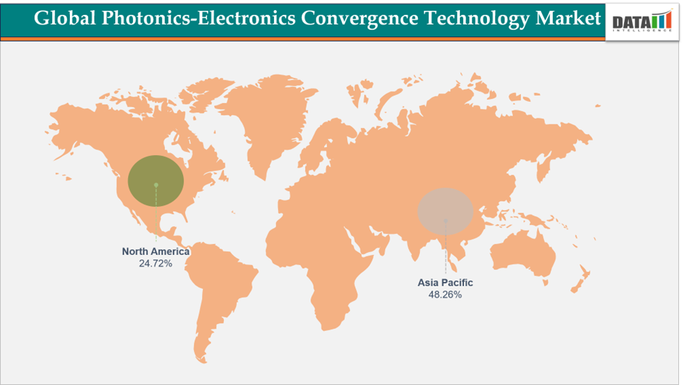
- Asia-Pacific holds 48.26% share, anchored by semiconductor manufacturing strength and infrastructure investments.
- Photonics Integrated Circuits (PICs) lead with 22.13% share, positioning them as the primary monetization layer.
- Data center energy demand projected to exceed 10% of global electricity consumption by 2030 is accelerating procurement of optical solutions.
- Government-backed semiconductor funding in the US alone exceeds USD 1.4 billion for packaging and optical interconnect programs, signaling long-term policy support.
- Venture and strategic investments in photonics startups and manufacturing localization indicate supply chain reshaping.
- Pricing and adoption trends show a shift from premium niche deployments to scalable integration through chiplets and advanced packaging.
Technology Shift and Demand Acceleration
AI and Data Center Power Economics Driving Adoption
The strongest Photonics Electronics Convergence Technology growth drivers originate from hyperscale data centers and AI infrastructure. Electrical interconnects are increasingly inefficient due to heat generation and signal loss. Optical interconnects deliver over 40% improvement in energy efficiency, directly impacting operating costs and sustainability metrics.
As AI models scale, chip-to-chip communication becomes the primary bottleneck. Photonics integration addresses this constraint by enabling high-bandwidth, low-latency data transfer across processors and memory layers.
Moore’s Law Slowdown and Node Migration Pressure
The deceleration of transistor scaling below 3nm is forcing semiconductor companies to explore heterogeneous integration. Photonics-electronics convergence complements advanced node migration by enabling performance gains without relying solely on transistor density.
This has elevated demand for:
- Silicon photonics interposers
- Chiplet architectures
- Optical I/O integration in processors
Telecom and 6G Infrastructure Readiness
Telecom operators are transitioning toward 6G-ready infrastructure requiring ultra-high-speed optical communication. Photonic transceivers and integrated circuits are becoming essential components in backbone and edge networks.
Supply Chain, Materials, and Packaging Landscape
The supply chain for photonics-electronics convergence technologies is evolving into a hybrid semiconductor-photonics ecosystem.
Wafer and Material Bottlenecks
Key materials include:
- Silicon photonics wafers
- Indium Phosphide (InP)
- Gallium Arsenide (GaAs)
- Lithium Niobate
Constraints in compound semiconductor fabrication and limited foundry capacity for photonics wafers are emerging as bottlenecks. These materials are critical for high-frequency and optical performance, particularly in telecom and defense applications.
Foundry and OSAT Ecosystem
The convergence market is reshaping the traditional semiconductor value chain:
- Foundries are integrating photonics capabilities alongside CMOS processes
- OSAT players are investing in advanced packaging for optical-electronic integration
- Hybrid integration techniques are enabling scalable manufacturing
GlobalFoundries’ investment in photonics packaging facilities highlights the transition toward volume production.
Advanced Packaging as a Differentiator
Advanced packaging technologies such as:
- 2.5D and 3D integration
- Silicon interposers
- Optical chiplets
are becoming critical for reducing latency and improving system performance. Packaging is no longer a backend process but a core innovation layer.
Market Opportunities and Investment Outlook
Semiconductor and Foundry Players
There is strong opportunity for semiconductor companies to capture value through integration of photonics into existing chip platforms. Companies that control both design and packaging layers are better positioned to scale.
Telecom and Data Infrastructure Providers
Telecom operators and hyperscalers are increasing procurement of optical interconnect solutions to reduce energy costs and enhance bandwidth. Investment cycles are aligned with AI infrastructure expansion.
Automotive and Defense Applications
Emerging demand from:
- Autonomous vehicles requiring high-speed sensor data processing
- Defense systems leveraging optical communication for secure, high-bandwidth transmission
is expanding the addressable market beyond traditional IT sectors.
Regional Manufacturing Expansion
Localization of photonics manufacturing, particularly in India and North America, presents opportunities for suppliers and equipment manufacturers.
Segmentation Analysis
Segmented by component (Photonics Integrated Circuits (PICs), Electronics Integrated Circuits (EICs), Optical Interconnects, Transceivers, Others), by material (Silicon Photonics, Indium Phosphide, Gallium Arsenide, Lithium Niobate, Others), by end-user (IT & Telecom, Consumer Electronics, Healthcare, Automotive & Mobility, Military & Defense, Industrial, Others), and by Region - Share, Trends, and Forecast to 2035.
Photonics Integrated Circuits (PICs)
PICs dominate the component segment with 22.13% market share, driven by their ability to integrate multiple optical functions on a single chip. Their application in AI processors, optical switching, and high-speed communication systems makes them central to future growth.
Electronics Integrated Circuits (EICs)
EICs remain critical for processing and control functions. Their integration with photonics enhances system performance across computing and telecom applications. Growth is tied to advancements in nanoelectronics and AI chip design.
End-User Insights
- IT & Telecom leads adoption due to data center and network infrastructure demand
- Automotive & Mobility is emerging with autonomous systems
- Military & Defense applications focus on secure and high-speed communication
Photonics Electronics Convergence Technology Regional Analysis
Asia-Pacific: Manufacturing Strength and Infrastructure Expansion
Asia-Pacific leads with 48.26% market share, supported by semiconductor manufacturing hubs and strong investment in AI, cloud computing, and telecom infrastructure. China and India are key contributors, focusing on scaling production and deploying optical technologies in data centers and networks.
North America: Fastest Growth Driven by Policy and Innovation
North America is the fastest-growing region, supported by government funding and private-sector innovation. The US leads with significant investments in semiconductor manufacturing, advanced packaging, and photonics R&D.
Programs under the CHIPS Act and private investments in silicon photonics are accelerating commercialization.
Europe: Strategic Focus on Sustainability and Research
Europe maintains a strong position in research and sustainable technology development. The region emphasizes energy-efficient photonics solutions and collaborative innovation across academia and industry.
Competitive Landscape and Company Strategies
The Photonics Electronics Convergence Technology top companies include:
- Intel Corporation
- NVIDIA Corporation
- STMicroelectronics
- Cisco Systems
- Marvell Technology
- Ciena Corporation
- Ayar Labs
- IPG Photonics
- NTT
- TDK Corporation
These companies are competing across multiple layers:
- Chip design and integration
- Optical component manufacturing
- Advanced packaging
- AI and telecom infrastructure solutions
Strategic focus areas include:
- Silicon photonics development
- Optical interconnect commercialization
- Partnerships with AI and data center companies
- Expansion into emerging markets
Collaborations and acquisitions are enabling companies to integrate photonics capabilities and scale production efficiently.
Recent Developments
In May 2026, Intel Corporation expanded its photonics-electronics convergence initiatives with advanced silicon photonics for high-speed data communication. The initiative focuses on improving bandwidth and energy efficiency. This supports next-generation data centers.
In April 2026, IBM Corporation introduced integrated photonics-electronics solutions for AI and high-performance computing systems. The development enhances processing speed and reduces power consumption. This benefits advanced computing applications.
In March 2026, Cisco Systems, Inc. strengthened its optical networking portfolio with photonic-electronic integrated technologies. The innovation focuses on scalable and high-capacity data transmission. This supports telecom infrastructure.
Pricing and Adoption Trends
Photonics Electronics Convergence Technology pricing and adoption trends indicate a gradual shift from high-cost niche deployments to scalable solutions enabled by:
- Chiplet architectures
- Standardized packaging
- Increased foundry participation
While initial costs remain high, long-term ROI is driven by reduced energy consumption and improved system performance, particularly in data centers and telecom networks.
Report Benefits
This report supports:
- Manufacturers in identifying product and integration strategies
- Investors in assessing high-growth segments and funding opportunities
- Suppliers in understanding material and component demand
- Technology companies in aligning with AI and telecom trends
- Procurement teams in evaluating cost-performance trade-offs
Target Audience
- Semiconductor manufacturers
- Photonics component suppliers
- Telecom operators
- Data center providers
- Automotive OEMs
- Defense contractors
- Investment firms and venture capitalists
- Technology strategy teams