Hybrid Bonding Market Size and Overview
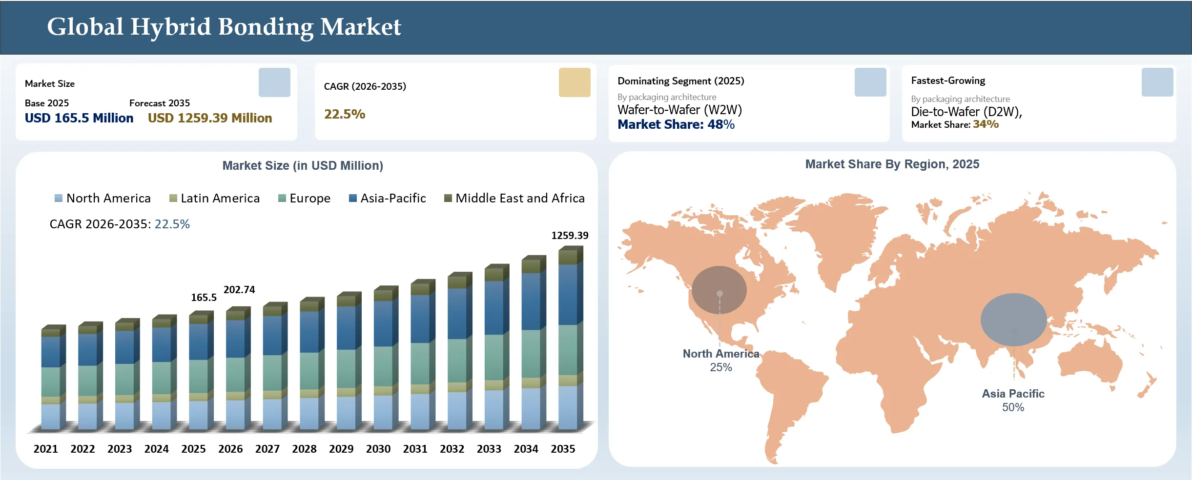
The global hybrid bonding market reached USD 165.5 million in 2025 and is expected to reach USD 1,259.39 million by 2035, growing with a CAGR of 22.5% during the forecast period 2026-2035. The market is emerging as a critical enabling technology for next-generation semiconductor integration, allowing direct copper-to-copper and dielectric bonding at ultra-fine pitches without the use of conventional micro-bumps. The technology is increasingly being adopted for HBM, AI accelerators, chiplets, advanced logic, 3D ICs, and CMOS image sensors, where higher bandwidth, lower power consumption, and improved interconnect density are essential. Industry collaboration is also accelerating technology commercialization; in 2025, Applied Materials acquired a 9% stake in BESI to strengthen joint development of integrated hybrid-bonding solutions for advanced semiconductor packaging. Additionally, Applied Materials is collaborating with EV Group (EVG) for wafer-to-wafer hybrid bonding and with BESI for die-to-wafer hybrid bonding solutions, highlighting the growing ecosystem around hybrid-bonding manufacturing.
The growing importance of hybrid bonding is further reflected in increasing investments by semiconductor equipment suppliers and memory manufacturers targeting AI-driven applications. In 2026, BESI reported a 104.5% increase in order bookings, supported by rising demand for hybrid-bonding solutions, particularly in high-bandwidth memory (HBM) applications for AI infrastructure. Industry qualification activities for next-generation HBM are also expanding, indicating that hybrid bonding is moving from niche adoption toward broader high-volume manufacturing. As semiconductor scaling becomes increasingly dependent on vertical integration and chiplet architectures, hybrid bonding is expected to play a foundational role in future advanced packaging and 3D semiconductor technologies.
White-Space Opportunities for Ultra-Fine-Pitch Hybrid Bonding and 3D Semiconductor Integration
Government funding is increasingly being directed toward advanced packaging infrastructure, creating an opportunity for suppliers of hybrid-bonding equipment and process technologies. The U.S. CHIPS National Advanced Packaging Manufacturing Program (NAPMP) has committed $300 million in 2024 through its first funding opportunity to support advanced substrates and materials research, including projects involving Applied Materials, Absolics, and Arizona State University. The program is designed to move advanced packaging technologies from R&D toward scalable domestic manufacturing, creating a stronger ecosystem for technologies such as hybrid bonding. In January 2025, the U.S. Department of Commerce also awarded up to $32 million to Corning and $18 million to Edwards Vacuum under the CHIPS program, demonstrating continued government support for the broader semiconductor equipment and packaging supply chain.
Corporate investment is also creating opportunities for higher-precision bonding technologies. In April 2025, Applied Materials acquired a 9% stake in BESI, making it BESI's largest shareholder; BESI is a leading supplier of advanced semiconductor packaging equipment and hybrid-bonding tools. The investment is particularly relevant because hybrid bonding is increasingly integrated with front-end semiconductor manufacturing processes, requiring closer coordination between wafer-processing and packaging equipment. In parallel, Micron announced a $10 billion investment over the next decade in a new U.S. research laboratory focused on future memory, computing, packaging, and semiconductor manufacturing technologies. Together, these investments indicate white-space potential for suppliers that can deliver ultra-fine-pitch bonding, high-accuracy alignment, surface preparation, metrology, and high-throughput equipment for next-generation HBM, 3D logic, and heterogeneous integration.
Hybrid Bonding Market Key Takeaways
- Asia-Pacific dominated the hybrid bonding market with an estimated 50% share in 2025, supported by its concentration of HBM, DRAM, NAND Flash, foundry, and advanced-packaging manufacturing capacity. North America followed with approximately 25%, supported by expanding advanced-packaging capabilities and increasing hybrid-bonding equipment commercialization.
- Wafer-to-Wafer (W2W) represented the dominant packaging architecture with an estimated 48% share in 2025, driven by its suitability for high-volume wafer-level integration across memory, CMOS image sensors, and 3D semiconductor architectures. Die-to-Wafer (D2W), with approximately 34% share, is expected to grow fastest, supported by HBM, chiplet integration, and heterogeneous packaging requirements.
- South Korea, Taiwan, Japan, and China remain the principal Asia-Pacific markets for hybrid bonding, supported by their established memory, foundry, semiconductor equipment, and advanced-packaging ecosystems. Increasing investment in HBM and 3D integration is shifting hybrid bonding from process development toward production qualification, particularly for high-density memory applications.
- North America's hybrid bonding adoption is being supported by equipment commercialization and advanced-packaging ecosystem development, with Applied Materials and BESI strengthening collaboration around integrated hybrid-bonding solutions. The combination of wafer processing, high-precision die placement, and bonding capabilities is supporting the transition toward high-volume manufacturing of advanced 3D semiconductor architectures.
Hybrid Bonding Market Industry Trends and Strategic Insight
- AI-driven HBM scaling is accelerating the transition toward hybrid bonding. Memory manufacturers are evaluating hybrid bonding as conventional micro-bump architectures face increasing pitch and stack-height constraints. SK hynix has indicated that hybrid bonding is being pushed toward HBM5, while Samsung is developing next-generation hybrid-bonding-based HBM architectures.
- Die-to-wafer and wafer-to-wafer architectures are expanding beyond memory into 3D logic and chiplet integration. Tokyo Electron's 2026 technology roadmap identifies hybrid/fusion bonding for HBM, 3D ICs and logic disaggregation, with die-to-wafer and wafer-to-wafer approaches progressing from R&D toward high-volume manufacturing.
- Equipment suppliers are increasingly integrating bonding with upstream and downstream process steps. Applied Materials introduced new CMP, deposition and eBeam systems in June 2026 specifically targeting higher-yield HBM and logic stacking, reflecting the growing importance of surface planarity, process control and defect inspection alongside the bonding step itself.
- Hybrid bonding is moving closer to production-scale qualification. BESI reported that its hybrid-bonding customer base increased from 15 customers at the end of 2025 to 21 in Q2 2026, covering logic, memory, co-packaged optics and consumer electronics. Its Q2 2026 orders also reached €292.9 million, more than twice the level recorded a year earlier, highlighting strong demand for advanced packaging technologies.
Hybrid Bonding Market Scope
| Metrics | Details | |
| 2025 Market Size | USD 165.5 Million | |
| 2035 Projected Market Size | USD 1,259.39 Million | |
| CAGR (2026-2035) | 22.5% | |
| Largest Market | Asia-Pacific | |
| Fastest Growing Market | North America | |
| By Bonding Type | Copper-to-Copper (Cu-Cu), Copper-to-Pad/Metal-to-Pad, Others | |
| By Packaging Architecture | Wafer-to-Wafer (W2W), Die-to-Die (D2D), Die-to-Wafer (D2W) | |
| By Wafer Size | 200 mm, 300 mm, Other Wafer Sizes | |
| By Integration Level | 2.5D Packaging, 3D Stacked ICs, Heterogeneous Integration | |
| By Process Flow | Front-end, Back-end | |
| By Bonding Orientation | Face-to-Face (F2F), Face-to-Back (F2B), Back-to-Back (B2B) | |
| By Bond / Interconnect Pitch | >10 µm, 5–10 µm, 1–5 µm, <1 µm | |
| By Bonding Material | Cu-Cu, Cu-Dielectric, Dielectric-Dielectric, Hybrid Cu/Dielectric | |
| By Application | NAND Flash, DRAM, HBM, Advanced Logic & CPUs, GPUs & AI, Accelerators, HPC, 3D ICs & Chiplets, CMOS Image Sensors, Silicon Photonics & Co-Packaged Optics, Others | |
| By End-User | Consumer Electronics, IT & Telecommunications, Automotive, Industrial Automation, Healthcare & Medical, Aerospace & Defense, Others | |
| By Region | North America | U.S., Canada, Mexico |
| Europe | Germany, UK, France, Russia, Spain, Italy, Norway, Netherlands, Sweden, Denmark, Belgium, Switzerland, Austria, Poland, Finland, Rest of Europe | |
| Asia-Pacific | China, India, Japan, Australia, South Korea, New Zealand, Indonesia, Malaysia, Philippines, Singapore, Thailand, Vietnam, Rest of Asia-Pacific | |
| Latin America | Brazil, Argentina, Chile, Rest of Latin America | |
| Middle East and Africa | UAE, Saudi Arabia, South Africa, Israel, Egypt, Turkey, Qatar, Kuwait, Oman, Bahrain, Rest of Middle East and Africa | |
| Report Insights Covered | Competitive Landscape Analysis, Company Profile Analysis, Market Size, Share, Growth | |
Hybrid Bonding Market Disruption Analysis
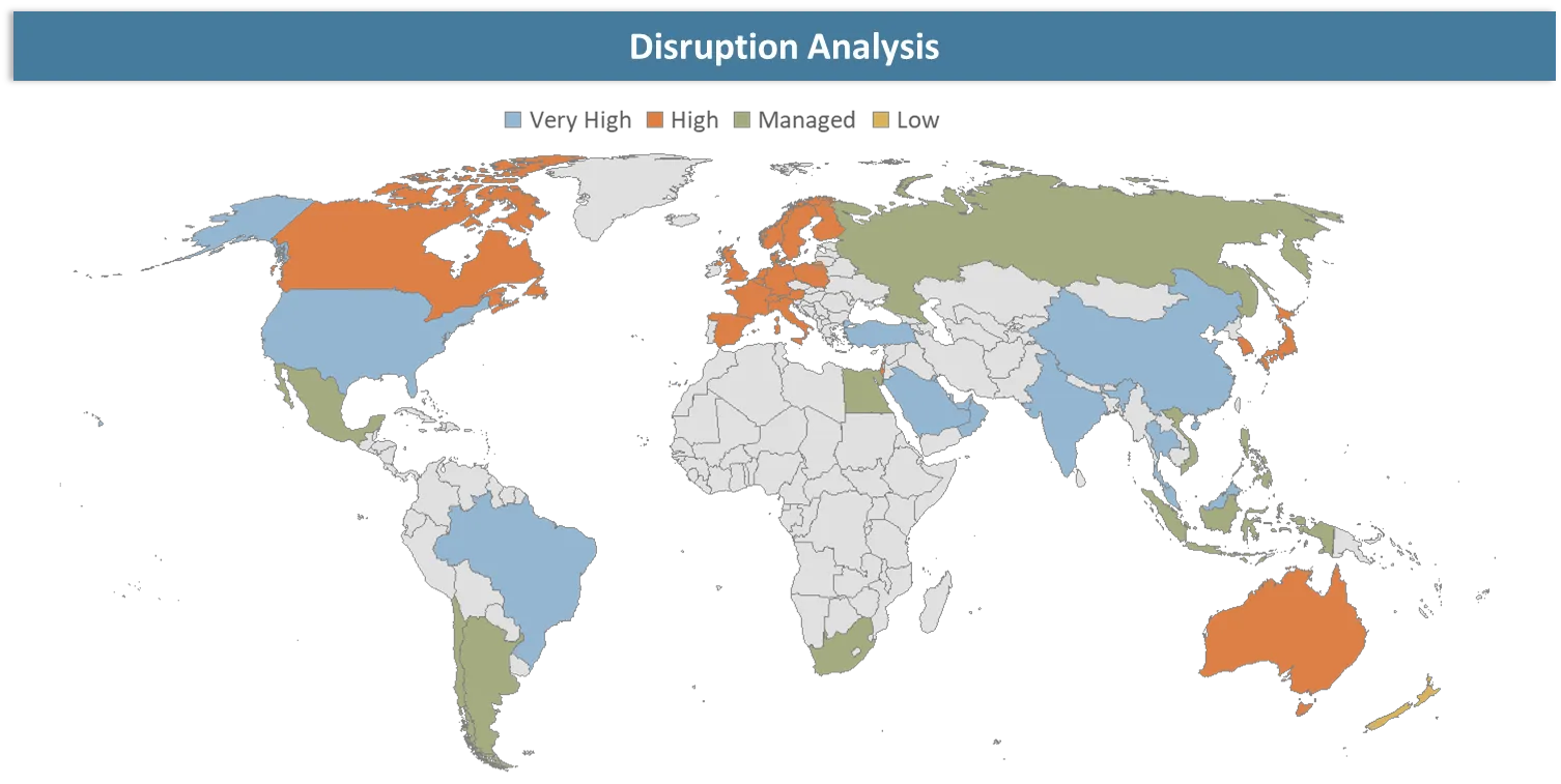
Shift from Micro-Bump Interconnects to Direct Hybrid Bonding
Hybrid bonding is disrupting conventional advanced-packaging architectures by replacing solder-based micro-bumps with direct copper-to-copper and dielectric-to-dielectric connections, enabling substantially denser vertical interconnects. In March 2026, a technical study by researchers from ETH Zurich, University of Bologna, and EPFL demonstrated wafer-on-wafer hybrid bonding as a pathway for improving communication performance in wafer-scale AI systems, reporting potential throughput improvements of up to 250%, latency reductions of up to 36%, and energy-per-byte reductions of up to 38% in the evaluated architectures.
In February 2026, EV Group (EVG) highlighted its hybrid and fusion bonding platforms at SEMICON Korea, including the GEMINI FB production wafer-bonding system, EVG 40 D2W overlay metrology system, and EVG 320 D2W die-preparation and activation system, targeting heterogeneous integration and advanced packaging. These developments indicate a shift toward direct, high-density die and wafer interconnection, creating competitive pressure on conventional bump-based approaches and increasing demand for hybrid bonding equipment capable of supporting advanced 3D semiconductor architectures.
Hybrid Bonding Market BCG Matrix: Company Evaluation
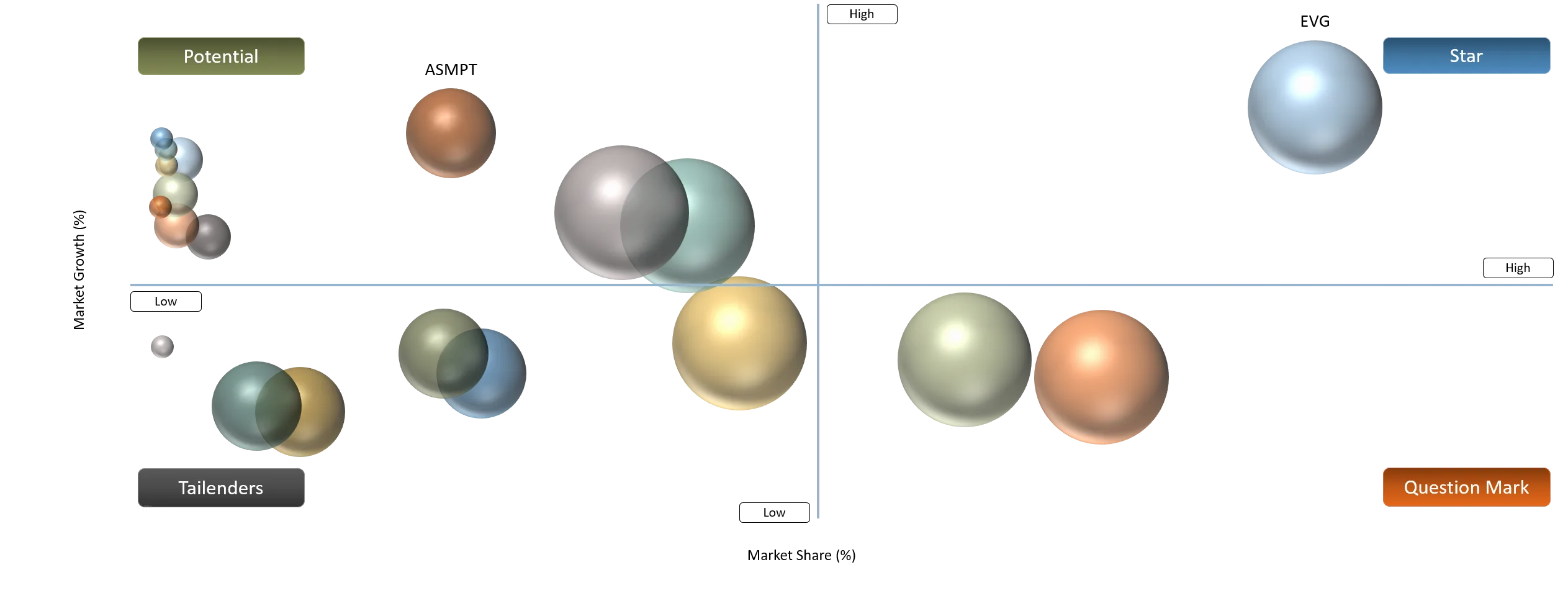
EV Group (EVG), BESI, SUSS MicroTec, and Applied Materials are positioned as Stars, supported by their established hybrid-bonding platforms and broader coverage of wafer-to-wafer, die-to-wafer, alignment, surface preparation, and process integration requirements. Potential players include Tokyo Electron, ASMPT, and Shibaura Mechatronics, leveraging established semiconductor process and advanced-packaging equipment capabilities that can be extended into hybrid-bonding production flows. Kulicke & Soffa and SET Corporation are positioned as Question Marks, with relevant bonding and advanced-packaging capabilities but comparatively narrower hybrid-bonding portfolios and market positioning.
HANMI Semiconductor is categorized as a Tailender within this equipment-focused peer set, as its bonding portfolio is more concentrated around specific advanced-memory and HBM applications rather than a broad hybrid-bonding process ecosystem. However, its HBM bonding capabilities provide a credible route to strengthen its position as hybrid bonding expands across high-density memory architectures. The competitive landscape is shaped by precision alignment, bonding throughput, wafer/die handling, surface conditioning, process integration, and scalability to high-volume manufacturing, with leading suppliers differentiating through increasingly integrated equipment platforms.
Hybrid Bonding Market Dynamics
Driver Impact Analysis
| Driver | Market Growth Impact (%) | Demand Concentration | Impacted Use Case | Strategic Impact |
AI workloads accelerate 3D integration and demand ultra-dense chip interconnects. | 25% | High demand concentration among AI accelerator, GPU, HPC, and advanced logic manufacturers developing high-density 3D architectures. | AI accelerators, GPUs, HPC processors, advanced logic, 3D ICs. | Accelerates adoption of hybrid bonding for ultra-fine-pitch interconnects, enabling higher bandwidth, lower interconnect distances, and greater vertical integration. |
HBM stacks require finer pitches, making hybrid bonding increasingly attractive. | 25% | Strong concentration among HBM and advanced memory manufacturers in Asia-Pacific and leading semiconductor production hubs. | HBM, DRAM, stacked memory, high-bandwidth AI memory systems. | Drives migration toward finer-pitch hybrid bonding as an alternative to conventional micro-bump interconnections, supporting higher memory density and bandwidth. |
Advanced chiplet architectures increase demand for direct high-density die interconnections. | 20% | Demand concentrated among advanced logic, processor, AI accelerator, and heterogeneous integration developers. | Chiplets, 3D ICs, advanced processors, heterogeneous integration. | Expands opportunities for die-to-wafer and die-to-die hybrid bonding, enabling shorter interconnects, higher interconnect density, and flexible multi-die architectures. |
Backside power delivery and logic scaling expand bonding adoption opportunities. | 15% | Concentrated among leading-edge logic and foundry manufacturers developing advanced transistor and power-delivery architectures. | Advanced logic, CPUs, GPUs, AI accelerators, backside power delivery. | Creates new bonding requirements for wafer stacking and advanced 3D integration, supporting continued demand for high-precision bonding and alignment equipment. |
Image sensors continue hybrid bonding adoption across stacked architectures globally. | 15% | Demand concentrated among CMOS image sensor manufacturers and consumer electronics, automotive, and industrial imaging applications. | CMOS image sensors (CIS), stacked image sensors, 3D image sensing. | Sustains hybrid bonding adoption beyond AI and memory by enabling compact stacked sensor architectures, higher pixel density, and improved device integration. |
AI Workloads Accelerate 3D Integration and Demand Ultra-Dense Chip Interconnects
The rapid scaling of AI computing is pushing semiconductor architectures toward higher-density 3D integration, where conventional interconnect approaches face increasing limitations. In June 2026, Applied Materials introduced new systems addressing DRAM and advanced packaging requirements, highlighting near-perfect surface planarity as critical for high-yield hybrid bonding. Applied Materials also identifies hybrid bonding as a key technology for connecting chips and wafers in heterogeneous integration, including 3D architectures supporting AI-related computing.
Equipment suppliers are therefore increasing their focus on high-precision hybrid bonding solutions that can support tighter interconnect pitches and complex multi-die structures. In May 2025, SUSS MicroTec introduced its XBC300 Gen2 die-to-wafer platform with post-bond accuracy below ±200 nm, targeting demanding 3D integration requirements. Besi is also positioning its hybrid bonding platform around optical alignment, cleanliness and high-density interconnects for next-generation advanced packaging. These developments indicate that AI-driven performance requirements are translating directly into investment in precision bonding, alignment and process-control capabilities.
Restraint Impact Analysis
| Restraint | Drag on Market Growth (%) | Primary Impact Area | Impacted Use Case | Strategic Impact |
Ultra-tight alignment requirements increase equipment complexity and manufacturing costs substantially. | 25% | Bonding accuracy, alignment systems, equipment complexity, and production costs | HBM, advanced logic, 3D ICs, chiplets, ultra-fine-pitch applications | Raises equipment investment and process-control requirements, increasing barriers to cost-effective high-volume hybrid bonding deployment. |
Bonding defects and contamination can reduce yields during high-volume manufacturing. | 25% | Yield, wafer cleanliness, defect control, and process reliability | HBM, DRAM, NAND Flash, advanced logic, CIS | Increases demand for advanced cleaning, surface preparation, inspection, and metrology, while extending qualification and ramp-up timelines. |
Capital-intensive bonding equipment limits adoption among smaller semiconductor manufacturers globally. | 20% | Capital expenditure, equipment acquisition, production scalability | Smaller-scale memory, logic, CIS, and advanced packaging manufacturers | Restricts adoption among smaller manufacturers and favors large semiconductor players with the capital and infrastructure required for high-volume hybrid bonding. |
Thermal expansion mismatches complicate reliable heterogeneous material integration at scale. | 15% | Thermal reliability, material compatibility, wafer stress, and bond integrity | Chiplets, 3D ICs, heterogeneous integration, advanced logic | Increases process-development and materials-engineering requirements, potentially limiting bonding reliability as heterogeneous architectures become more complex. |
Ultra-Tight Alignment Requirements Increase Equipment Complexity and Manufacturing Costs
Hybrid bonding is moving toward extremely tight overlay requirements, increasing the technical complexity of bonding equipment and the associated process infrastructure. In May 2026, imec and EV Group demonstrated 200 nm Cu interconnect pitch with below 40 nm post-bond overlay across 100% of dies on a 300 mm wafer. Achieving these required coordinated improvements in CMP, lithography corrections, pad design, and wafer-bonding equipment, illustrating that alignment cannot be addressed by the bonder alone.
The requirement for such precision increases the number of process-control and equipment capabilities needed for production, including high-accuracy alignment, thermal control, metrology, and closed-loop correction. SUSS currently specifies <100 nm overlay capability for its W2W platform, with integrated metrology and real-time X/Y/θ correction to maintain alignment during production. As pitch continues to shrink, manufacturers therefore face higher equipment complexity, tighter process windows, and greater qualification requirements, which can slow cost-efficient high-volume adoption of hybrid bonding.
Hybrid Bonding Market Segment Analysis
The global hybrid bonding market is segmented based on bonding type, packaging architecture, wafer size, integration level, process flow, bonding orientation, bond / interconnect pitch, bonding material, application, end-user, and region.
Die-to-Wafer Hybrid Bonding Gains Momentum Through Selective Die Stacking for HBM, Chiplets and 3D Integration
Die-to-wafer hybrid bonding is gaining momentum as advanced semiconductor architectures require selective stacking of known-good dies rather than wafer-level bonding alone. In May 2025, SUSS MicroTec introduced its XBC300 Gen2 D2W platform, targeting 200 mm and 300 mm substrates and supporting post-bond accuracy below ±200 nm. The platform integrates surface activation, die positioning and bonding within an automated workflow. Its development with SET Corporation specifically targets applications including 3D ICs and HBM. This reflects the industry's shift toward production-ready D2W solutions for increasingly complex heterogeneous integration.
D2W is particularly relevant where dies with different functions, process nodes or specifications need to be selectively integrated onto a common substrate. EV Group's 2026 technology portfolio positions D2W hybrid bonding as an enabler for chiplet integration, HBM stacks and 3D SoC integration, while its process flow covers die preparation, cleaning, activation, collective die transfer and high-precision alignment. These capabilities address the requirements of advanced memory and heterogeneous computing architectures. As manufacturers move toward greater vertical integration, D2W provides equipment suppliers with opportunities across bonding, die handling, surface preparation, metrology and alignment.
Hybrid Bonding Market Geographical Penetration
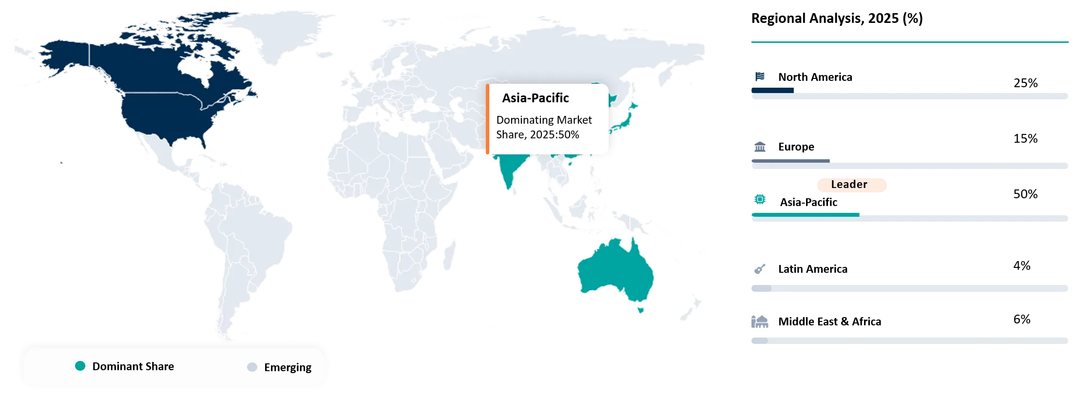
Advanced Packaging Localization Accelerates Hybrid Bonding Opportunities in North America
North America is strengthening its position in hybrid bonding through government-backed development of a domestic advanced-packaging ecosystem. In January 2025, the U.S. Department of Commerce finalized USD 1.4 billion in CHIPS National Advanced Packaging Manufacturing Program (NAPMP) awards, intended to establish a self-sustaining, high-volume domestic advanced-packaging industry. The program covers technology development, prototyping and pilot-scale manufacturing rather than focusing only on conventional assembly. This creates an important commercialization pathway for 2.5D/3D integration and high-density interconnect technologies. The development also improves the addressable opportunity for suppliers of bonding, alignment, metrology and process equipment.
The regional ecosystem is further supported by the USD 300 million NAPMP award to Absolics, Applied Materials and Arizona State University for advanced substrate and material R&D. The objective is to validate technologies and transition them toward U.S. manufacturing at scale, strengthening the materials and process infrastructure surrounding advanced packaging. For hybrid bonding, this ecosystem is important because high-density bonding requires coordinated development across surfaces, materials, equipment and process control. Consequently, North America is developing from primarily a technology-development market into a more complete advanced-packaging manufacturing ecosystem.
U.S. Hybrid Bonding Market Trends
The U.S. is directly contributing to hybrid-bonding commercialization through the activities of Applied Materials, which has developed an integrated equipment approach with BESI. In April 2025, Applied Materials announced that the two companies had co-developed an integrated hybrid-bonding system combining front-end wafer and chip processing with high-speed, high-accuracy die placement and interconnect capabilities. The companies positioned the solution specifically for taking hybrid bonding into very high-volume manufacturing. This is directly relevant to the U.S. equipment ecosystem because Applied Materials is integrating hybrid bonding into its broader semiconductor manufacturing platform.
The technology is also moving toward production-level adoption rather than remaining confined to laboratory development. In November 2025, the Applied Materials-BESI Kinex system was reported as one of the early hybrid-bonding platforms demonstrated in high-volume production, with the companies continuing to target improvements in accuracy, speed and flexibility. The development is strategically important because manufacturing-scale hybrid bonding requires coordinated wafer processing, die placement, alignment and bonding rather than a standalone bonder. This strengthens the U.S. opportunity across equipment integration and process-control technologies.
Canada Hybrid Bonding Market Outlook
Canada is developing an advanced semiconductor packaging ecosystem through major investment in the IBM Canada and C2MI infrastructure in Bromont, Quebec. In November 2025, the Canadian government announced up to CAD 210 million toward a CAD 662 million IBM Canada-C2MI project to expand semiconductor packaging, post-processing and commercialization capabilities. The project is intended to strengthen Canada's position in advanced semiconductor manufacturing and support applications associated with AI and high-performance computing. Expansion of these facilities increases regional demand for sophisticated packaging processes and supporting equipment. It also provides a domestic environment for qualification of increasingly complex semiconductor integration technologies.
The Canadian ecosystem is complemented by specialized semiconductor R&D infrastructure that can support advanced interconnect development. The IBM Canada-C2MI investment expands capabilities across packaging and post-processing rather than limiting development to front-end wafer fabrication. This is strategically relevant because hybrid bonding requires close coordination between semiconductor fabrication, die preparation, packaging and testing. As Canada's semiconductor ecosystem expands, suppliers can potentially participate through equipment, materials, process-development and integration partnerships. The country's role is therefore more likely to develop as a specialized advanced-packaging and R&D hub rather than as a high-volume global memory manufacturing center.
HBM and Next-Generation Wafer Bonding Accelerate Regional Hybrid Bonding Adoption in Asia-Pacific Market Growth
Asia-Pacific has the strongest direct application linkage because major memory and semiconductor manufacturers are actively developing bonding technologies for next-generation stacked architectures. In August 2026, Samsung Electronics presented its zHBM roadmap, describing next-generation wafer-bonding technology capable of achieving more than 10× the memory density of HBM5, while targeting approximately 3× higher energy efficiency and more than 50% lower thermal resistance. Samsung also projected approximately eight times the performance of HBM5 for the associated interface system. This directly connects wafer-bonding technology with the region's HBM and AI-memory development roadmap.
China is also developing a direct hybrid-bonding application pathway through memory-industry collaboration. In 2025, YMTC and CXMT established a strategic collaboration to accelerate domestic HBM development, combining CXMT's DRAM capabilities with YMTC's hybrid-bonding technology developed for 3D NAND. The collaboration is intended to combine memory and bonding expertise for domestic HBM production. This demonstrates that hybrid bonding is becoming strategically relevant not only to established HBM manufacturers but also to emerging Asian memory ecosystems seeking higher-density stacked memory architectures
Japan Hybrid Bonding Market Trends
Japan's direct hybrid-bonding opportunity is closely connected with advanced chip stacking and semiconductor process development rather than HBM alone. TSMC's Japan-based manufacturing ecosystem is incorporating advanced packaging expertise, while its SoIC platform uses an innovative bonding scheme to scale bond pitch below 10 µm for high-density die-to-die interconnects. TSMC reports that its 3 nm chip-stacking technology entered volume production in 2025, demonstrating the transition of fine-pitch bonding technologies into commercial advanced-logic applications. This creates a direct technology linkage between Japan's semiconductor manufacturing ecosystem and high-density bonding requirements.
Japan also benefits from its established semiconductor-equipment and materials ecosystem, which is relevant because hybrid bonding requires extremely tight control over surface preparation, alignment, contamination and wafer processing. The increasing use of fine-pitch chip stacking creates opportunities for Japanese suppliers participating in these enabling processes. Rather than characterizing Japan primarily as an HBM market, it is more appropriate to position the country around advanced logic, 3D integration, materials and precision semiconductor equipment, where fine-pitch bonding technologies are increasingly relevant.
South Korea Hybrid Bonding Market Trends
South Korea represents one of the strongest application environments for hybrid bonding because of its concentration in HBM and advanced memory manufacturing. In April 2026, SK hynix broke ground on its P&T7 advanced-packaging facility in Cheongju, expanding its infrastructure for next-generation AI memory packaging. The facility is part of SK hynix's broader effort to increase advanced packaging capacity alongside its HBM production capabilities. The development directly strengthens the country's back-end semiconductor ecosystem and creates additional requirements for high-precision bonding and process-control equipment. It also reinforces South Korea's role as a major qualification market for advanced memory packaging technologies.
The investment momentum increased further in 2026, with SK hynix outlining a KRW 100 trillion investment for its Cheongju semiconductor operations, including KRW 20 trillion for the P&T7 advanced-packaging facility. The company's wider Korean investment program covers HBM, DRAM, NAND and advanced packaging, creating demand across multiple semiconductor manufacturing stages. For hybrid-bonding equipment suppliers, this provides a particularly attractive environment because HBM requires increasingly dense vertical interconnection and tighter packaging integration. South Korea consequently represents a high-priority market for suppliers targeting HBM-oriented bonding, die handling, alignment and advanced-packaging equipment.
Hybrid Bonding Market Competitive Landscape
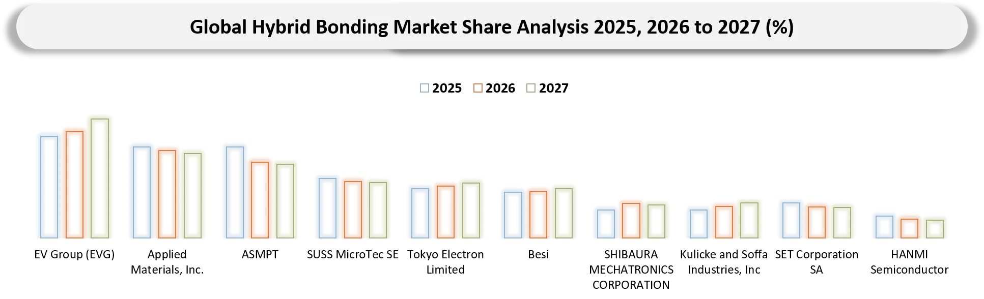
- Key players include EV Group (EVG), Applied Materials, Inc., ASMPT, SUSS MicroTec SE, Tokyo Electron Limited, Besi, SHIBAURA MECHATRONICS CORPORATION, Kulicke and Soffa Industries, Inc, SET Corporation SA, HANMI Semiconductor.
Key Developments
- March 2026: Kulicke & Soffa Industries, Inc. expanded its memory solutions portfolio to include advanced thermo-compression and Hybrid Bonding technologies, with its hybrid-bonding program having accelerated since 2024. The company said the solutions target emerging HBM, high-bandwidth flash, and high-density DRAM architectures and reported early customer interest.
- April 2026: HANMI Semiconductor announced plans to launch a second-generation hybrid bonder by the end of 2026, targeting next-generation HBM applications. The development represents an expansion from its established thermo-compression bonding portfolio toward hybrid bonding for higher-density memory packaging.
- June 2026: Applied Materials introduced new CMP, deposition, and eBeam systems for advanced packaging, explicitly identifying its new Opta Quad CMP platform as particularly important for hybrid bonding, where near-perfect surface planarity is required for high-yield bonding. The systems target higher-yield HBM and logic chip stacking.
- May 2025: SUSS MicroTec introduced its XBC300 Gen2 D2W hybrid-bonding platform, supporting 200 mm and 300 mm substrates with post-bond accuracy below ±200 nm. Developed with bonding specialist SET Corporation, the system offers up to 40% space savings compared with other fully integrated D2W hybrid-bonding solutions.
- April 2025: Applied Materials acquired a 9% stake in BESI, becoming the Dutch advanced-packaging equipment company's largest shareholder. The transaction strengthened cooperation between Applied Materials' wafer-processing capabilities and BESI's hybrid-bonding technology, supporting development of advanced packaging solutions for high-volume semiconductor manufacturing.
- April 2026: BESI reported quarterly order bookings of €269.7 million, up 104.5% year over year, with the company identifying particularly strong demand for hybrid bonding. Reuters also reported that a second customer had begun qualification of BESI's technology for high-bandwidth memory, indicating progression toward broader HBM adoption.
- April 2026: SK hynix reportedly completed validation of a 12-high HBM structure using hybrid bonding, while working to improve yields before mass production. The company reportedly ordered an Applied Materials–BESI inline hybrid-bonding system costing approximately KRW 20 billion, marking its first reported acquisition of hybrid-bonding equipment intended for mass production.
- August 2026: SK hynix highlighted hybrid bonding as a potential foundational technology for future semiconductor architectures, noting its relevance to next-generation HBM, DDR6+, backside power delivery, high-bandwidth flash, and heterogeneous integration. The company identifies HBM as a particularly promising application because conventional thermo-compression bonding faces increasing limitations at very fine pitches and higher stack heights.
Key Procurement Priorities and Buyer Evaluation Criteria
- Bonding accuracy and yield performance are the primary procurement considerations, as buyers evaluate sub-micron alignment, overlay control, void formation, contamination and bonding uniformity. These parameters directly influence yield when supporting fine-pitch HBM, 3D IC and chiplet applications.
- Throughput and manufacturing scalability are also critical, with semiconductor manufacturers assessing wafers/dies per hour, cycle time, equipment uptime and automation. Buyers increasingly prefer platforms capable of supporting high-volume production across 200 mm and 300 mm wafers.
- Process flexibility and integration influence equipment selection, particularly compatibility with W2W, D2W and D2D architectures alongside plasma activation, surface preparation and metrology. The ability to support 1-5 µm and sub-1 µm pitches is becoming increasingly important for next-generation applications.
- Total cost of ownership and supplier support remain key commercial criteria, covering equipment cost, maintenance, consumables, service response and process-development support. Buyers also assess the supplier's technology roadmap to ensure equipment can accommodate higher stack counts, finer pitches and future HBM and advanced-logic requirements.
Why Choose DataM?
- Technological Innovations: Evaluates advancements in hybrid bonding technologies, including Cu-Cu bonding, dielectric bonding, ultra-fine-pitch interconnects, D2W/W2W platforms, high-precision alignment, surface activation, metrology, and automated bonding systems that enable higher-density HBM, 3D IC, chiplet, and advanced-logic integration.
- Product Performance & Market Positioning: Assesses hybrid-bonding equipment and solutions based on bonding accuracy, overlay control, throughput, defect rates, yield performance, wafer/die compatibility, pitch capability, automation, and process integration, highlighting how suppliers differentiate across high-volume memory and advanced-logic manufacturing.
- Real-World Evidence: Highlights commercial adoption, customer qualification, technology demonstrations, equipment installations, and production deployments of hybrid bonding across HBM, DRAM, NAND Flash, 3D ICs, chiplets, advanced logic, and CMOS image sensors, demonstrating improvements in interconnect density, thermal performance, bandwidth, and integration efficiency.
- Market Updates & Industry Changes: Tracks hybrid-bonding equipment launches, HBM qualification programs, strategic investments, technology partnerships, manufacturing expansions, process-development initiatives, and advances in fine-pitch bonding across North America, Asia-Pacific, Europe, and other semiconductor manufacturing hubs.
- Competitive Strategies: Analyzes how leading companies strengthen their positions through equipment innovation, strategic partnerships, acquisitions, technology collaborations, customer qualification, production-scale deployments, and integration of bonding with surface preparation, metrology, alignment, and wafer-processing capabilities.
- Pricing & Market Access: Examines equipment pricing and procurement considerations based on bonding architecture, wafer size, throughput, alignment accuracy, pitch capability, automation level, process integration, and customization requirements, alongside purchasing channels involving semiconductor equipment manufacturers, foundries, IDMs, OSATs, and memory manufacturers.
- Market Entry & Expansion: Identifies opportunities created by increasing HBM layer counts, AI accelerators, chiplet architectures, 3D logic, backside power delivery, and ultra-fine interconnect requirements, while evaluating strategies including regional expansion, technology partnerships, application-specific platforms, customer co-development, and high-volume manufacturing qualification.
Target Audience
- Semiconductor IDMs & Memory Manufacturers
- Foundries & Advanced Logic Manufacturers
- OSATs & Advanced Packaging Providers
- Semiconductor Equipment Manufacturers
- Semiconductor Materials & Process Suppliers
- AI, HPC & Accelerator Chip Designers
- Advanced Packaging R&D Institutes & Research Organizations
- EDA, Semiconductor Design & IP Companies
- Investment & Corporate Strategy Teams
- Government & Semiconductor Policy Organizations