Chiplet market Size
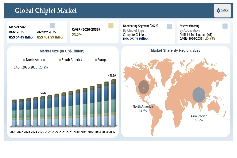
The global chiplet market Size reached US$ 54.49 billion in 2025 and is expected to reach US$ 431.99 billion by 2035, growing with a CAGR of 23.2% during the forecast period 2026-2035.
The market is witnessing rapid expansion as semiconductor manufacturers increasingly adopt chiplet-based architectures to overcome the cost, yield and scalability limitations of monolithic integrated circuits at advanced process nodes. According to the World Semiconductor Trade Statistics (WSTS), the global semiconductor industry has generated revenues of US$791.7 billion in 2025 while the global capital expenditure on semiconductors stood at US$186.9 billion.High demand for semiconductor solutions for artificial intelligence, HPC, cloud and automotive applications will fuel growth in the use of chiplets-based processors.
Commercialization of the cutting-edge packaging technologies like 2.5D, 3D, CoWoS and EMIB, coupled with UCIe as an accepted standard in the industry, is bringing about heterogeneous integration and scalability to multi-die architecture. According to the Semiconductor Industry Association (SIA), the global market for AI semiconductors exceeded US$200 billion in 2025, whereas High Bandwidth Memory (HBM) exceeded US$30 billion in yearly revenues, signifying the rising significance of chiplet-enabled computing platforms. These advancements, combined with increasing investments in reusable chiplet IP and advanced packaging capacity, are positioning chiplets as a foundational architecture for next-generation AI, data center, networking and edge computing applications.
Chiplet Market Key Takeaways
- Asia-Pacific region dominated the chiplet market Share holding 35.9% of the global chiplet market in 2025 due to the presence of semiconductor foundry, advanced packaging operations and electronics manufacturing facilities in Taiwan, South Korea, China and Japan.
- North America region captured 34.3% of the global chiplet market Share in 2025 on account of presence of leading fabless semiconductor companies, hyperscale cloud companies along with continuous investments in AI accelerator chips and HPC chips.
- Compute Chiplets represented 46.0% of the global chiplet market in 2025 owing to rising demand for AI processors, GPUs, CPUs and HPC accelerators that need to be made in multi-die architectures.
- The Artificial Intelligence (AI) application segment is expected to grow at a CAGR of 25.7% in the period 2026–2035, supported by rapid investments in generative AI infrastructure, hyperscale data centers and next-generation AI accelerators.
- Growing adoption of 2.5D and 3D advanced packaging, High-Bandwidth Memory (HBM) integration and the Universal Chiplet Interconnect Express (UCIe) standard is accelerating commercialization and enabling next-generation AI, data center, automotive and networking processors.
Chiplet Industry Trends and Strategic Insights
- Rapid Standardization Through UCIe Adoption: Widespread use of the UCIe, Universal Chiplet Interconnect Express, is creating a common interconnect standard for connecting dies in a chiplet ecosystem from multiple vendors, making it easier to design chiplets from different manufacturers and building an open chiplet ecosystem.
- Transitioning to Heterogeneous Multiple-Node Chiplet Ecosystems: Companies operating in semiconductor sector are increasingly designing systems that include heterogeneous chiplets that consist of compute, memory, IO and accelerator dies fabricated using multiple processes into one package.
- Scaling of Packaging Capacity: Major foundries and packaging companies have been investing significantly in capacity related to 2.5D, 3D, fan-out and SIP packages to fulfill the increasing needs for AI processor, high-performance computing and datacenter systems using chiplets.
- Growing Adoption of Domain-Specific Chiplets: Chiplet technology is being used to develop chiplets which are customized specifically for different applications like AI accelerators, network processors, automobile platforms, edge computing applications and telecommunication equipment.
- Emergence of Reusable Chiplet IP and Multi-Vendor Ecosystems: Industry is working towards making modular semiconductor development possible with the help of the above -mentioned technology trends.
Chiplet Market Scope
| Metrics | Details | |
| 2025 Market Size | US$ 54.49 Billion | |
| 2035 Projected Market Size | US$ 431.99 Billion | |
| CAGR (2026-2035) | 23.2% | |
| Largest Market | Asia-Pacific | |
| Fastest Growing Market | Asia-Pacific | |
| By Chiplet Type | Compute Chiplets, Memory Chiplets, I/O Chiplets, Analog & Mixed-Signal Chiplets, RF Chiplets, Photonic Chiplets, Security Chiplets, Power Management Chiplets and Others | |
| By Packaging Technology | 2D Packaging, 2.5D Packaging, 3D Packaging, Fan-Out Packaging, Bridge-Based Packaging (EMIB and Similar), Multi-Chip Module (MCM), System-in-Package (SiP) and Others | |
| By Interconnect Standard | Universal Chiplet Interconnect Express (UCIe), Bunch of Wires (BoW), OpenHBI, Proprietary Interconnects and Others | |
| By Substrate | Silicon Interposer, Organic Substrate, Glass Substrate, Embedded Bridge Substrate, Ceramic Substrate and Others | |
| By Integration Type | Homogeneous Chiplets and Heterogeneous Chiplets | |
| By Application | Artificial Intelligence (AI), High-Performance Computing (HPC), Data Centers & Cloud Computing, Consumer Electronics, Automotive, Telecommunications, Industrial, Aerospace & Defense, Healthcare and Others | |
| By End-User | Integrated Device Manufacturers (IDMs), Fabless Semiconductor Companies, Foundries, Outsourced Semiconductor Assembly & Test (OSAT) Providers, Original Equipment Manufacturers (OEMs), Cloud Service Providers, Research Institutions & Government Organizations and Others | |
| By Region | North America | U.S., Canada, Mexico |
| Europe | Germany, UK, France, Spain, Italy, Poland | |
| Asia-Pacific | China, India, Japan, Australia, South Korea, Indonesia, Malaysia, Singapore, Vietnam, Thailand, Philippines, Taiwan | |
| South America | Brazil, Argentina | |
| Middle East and Africa | UAE, Saudi Arabia, South Africa, Israel, Turkiye | |
| Report Insights Covered | Competitive Landscape Analysis, Company Profile Analysis, Market Size, Share, Growth | |
Why does this report matter in 2026?
The chiplet market will reach a crucial juncture in 2026 as advancements in AI, HPC and the deployment of hyperscale cloud services will drive the evolution of modular architectures for semiconductors. Increased usage of advanced packaging and Heterogeneous Integration (HI), High Bandwidth Memory (HBM) and Universal Chiplet Interconnect Express (UCIe) is allowing semiconductor vendors to address the economic and technical challenges associated with monolithic semiconductor chips by offering high performance, greater energy efficiency and faster innovations. With an increasing investment in AI and semiconductor fabrication, chiplets are poised to be the building blocks of future computing platforms.
The report provides intelligence in understanding market dynamics, technological developments, competitive strategies and growth opportunities in the chiplet market. The report studies various aspects such as market segments, regional activities, activities from various companies and ecosystem partnership trends that allow semiconductor manufacturers, foundry players, OSATs, technology players, venture capitalists and other stakeholders in the ecosystem to gain an edge over competition and identify lucrative opportunities in the market.
Chiplet market White Space & Investment Opportunities
- Commercializing Open Chiplet Platforms: Increased acceptance of UCIe and reusable IP chiplets provides growth prospects in the domain of open chiplet platforms, licensing third-party IPs and multi-vendor semiconductor ecosystems.
- Development of Advanced Packaging Technology: The increasing usage of CoWoS, SoIC, EMIB, 2.5D/3D Packaging technology and fan-out wafer provides growth opportunities in foundry, outsourced assembly/test suppliers, Packaging substrate and manufacturing capabilities.
- Next Generation AI and HPC Chiplet Solutions: With increasing adoption of AI processors, hyperscale cloud and HPC, there is a substantial growth prospect with respect to development of compute, HBM and application-specific chiplets.
- Chiplets in Automotive and Edge Computing Platform: The rise in utilization of chiplets in autonomous vehicles, ADAS, industry automation, robotic and edge AI systems is a lucrative market for domain-specific chipsets.
- EDA, Design Automation and Verification of Chiplet Designs: Growing design complexity with regard to multi-die designs is resulting in opportunities in EDA tools and verification technologies.
Chiplet Future Market Transformation
The future of the Chiplets Market will be shaped by the mass-scale shift in semiconductor companies from their traditional approaches based on monolith semiconductors to new designs built on the foundation of multi-die, heterogeneous structures, which will bring about greater scalability, enhanced performance and efficiency in manufacturing. Development in die-to-die interfaces (for instance, UCIe), reusable IP blocks of chiplets, along with innovations in packaging technologies such as 2.5D, 3D, CoWoS and SoIC, will allow semiconductor firms to build more complex processors and do so with lower costs of development, better yields and accelerated time to market. With the growth of AI, HPC and hyperscale cloud computing, chiplet-based architectures will gain popularity.
Future advancements in this domain are likely to focus on interoperability in an ecosystem of chiplets, which allows the use of pre-integrated and easily reusable chiplets from multiple suppliers to be packaged together to enable more rapid production and flexibility in design capabilities. Enhanced collaboration between semiconductor producers, semiconductor fabricators, outsourced assembly and test partners, intellectual property providers and cloud computing providers will help hasten the realization of the latest solutions based on chiplets in areas such as automotive, telecommunications, industrial, consumer electronics and AI at the edge segments of the market.
Chiplet market Buyer Decision-Making Criteria
Organizations which invest in semiconductor technologies relying on chiplets assess suppliers by their capability to provide them with high-performance and cost-effective architectures for future computing workloads. When making purchase decisions, organizations take into consideration technical competencies of the suppliers, availability of ecosystems for integration into, production maturity, long-term supply assurance, as well as opportunities to speed up product development processes. With increasing use in AI, HPC, datacenters, automotive, telecommunication and industrial spheres, the list of criteria becomes even longer.
Major Buyer Decision-Making Criteria
- Compute Performance and Power Efficiency
- Interoperability and Ecosystem Compatibility
- Advanced Packaging and Integration Capabilities
- Manufacturing Quality, Yield and Reliability
- Supply Chain Stability and Production Capacity
- Total Cost of Ownership (TCO) and Time-to-Market
- Scalability and Customization Flexibility
- Vendor Innovation Roadmap and Technical Support
Chiplet market Economic & Investment Analysis
The chiplet market is attracting substantial capital investment as semiconductor manufacturers seek cost-effective alternatives to increasingly expensive monolithic chip development at advanced process nodes. Higher capital expenditures being invested in advanced packaging solutions such as CoWoS, SoIC, 2.5D and 3D packaging solutions have increased production capacity for applications such as AI accelerators, high performance computing (HPC) and large data centers processor chips. In addition to that, semiconductor incentive programs and local production initiatives by governments have promoted investments in semiconductor chiplets.
In addition, there have been increased investments across the chiplet ecosystem via collaborations, venture capital funding and companies' investments in reusable chiplet intellectual property (IP), die-to-die interconnections technology, EDA software and heterogeneous integration solutions. Chiplet architecture promises higher ROI due to increased manufacturing efficiencies and lower costs, which allow for quicker commercialization of specific-purpose processors. Given the increasing demand for semiconductors in AI-based applications, there will be continuous investments in designing, packaging, manufacturing and overall ecosystem development.
Chiplet Investment Trends in the Market
- Increased Spending on Advanced Packaging Capabilities: Semiconductor, foundry and OSAT suppliers have been increasing their investment levels in terms of CoWoS, SoIC, 2.5D, 3D and fan-out packaging for manufacturing many chiplets.
- Funding on AI and HPC Chiplet Platforms: The high demand for AI accelerators, cloud-based computing solutions and HPC is encouraging funding for compute chiplets, High Bandwidth Memory (HBM) and heterogeneous integration technologies.
- Increased Spending on Chiplet IP and EDA Tools: There has been increased investment by venture capitalists and semiconductor vendors in chiplet IP reuse, EDA tooling and verification for multiple dies and chiplets.
- Investments in Strategic Open Chiplets Ecosystems: Participants in the industry are making strategic investments in interconnect technologies based on UCIe, interoperable chiplets and ecosystems in order to facilitate multi-vendor integration and commercialization.
- Expansion through M&A and Strategic Alliances: Companies are making acquisitions and joint ventures in addition to forming long-term technology alliances with other companies for expanding their chiplets and other capabilities.
Strategic Indicators For the chiplet market
High Regulation Impact
The chiplet market is increasingly influenced by evolving semiconductor regulations, export controls, intellectual property (IP) protection frameworks and government policies supporting domestic semiconductor manufacturing and advanced packaging. The impact of regulations controlling the international flow of the latest semiconductor products and technologies and the government incentive policies related to manufacturing and advanced packaging facilities within the territory of countries is affecting the market trends. Since chiplet architectures are becoming a part of the AI and HPC markets, regulations will have even more impact on the market.
High Investment Activity
The chiplet market is experiencing high investment activity as companies prioritize long-term technology leadership and ecosystem expansion over incremental semiconductor innovation. Investment is primarily targeted at the creation of reusability for chiplet platforms, design tool extension, advancement of die-to-die connectivity and building chiplet ecosystem that allows rapid product development and multi-vendor integration. On the other hand, strategic investment, partnership deals and company acquisition facilitate the maturity of the chiplet ecosystem, thus confirming its importance as the field of investment in the world semiconductor industry.
Supply Chain Disruption
The chiplet market is still vulnerable to supply chain interruptions owing to the reliance on a few sources for advanced packaging substrates, high bandwidth memory (HBM), state-of-the-art foundries and customized semiconductor equipment. Changes in the availability of raw materials, longer procurement cycles for advanced packaging components and concentration of essential manufacturing capabilities at a few major suppliers worldwide can result in production delays and higher costs. This trend has prompted semiconductor firms to explore diversified source options, develop stronger supplier relationships, localize production processes and create long-term purchase agreements.
Pricing Volatility
The chiplet market is known for its unstable pricing because of the high prices of the best quality semiconductor production methods, the advanced packaging method and the integration of High-Bandwidth Memory (HBM). The processing of chips making use of 3 nm process nodes can cost more than $ 20,000 per wafer. The advanced packaging technologies, such as 2.5D and 3D integrated, make the costs of complicated multi-die semiconductor devices higher. Prices for silicon wafers, the advanced substrates, HBM and OSAT services make variations in manufacturing and ultimately the prices of chiplets..
As an effort to deal with the risks associated with uncertain pricing, the companies producing semiconductor components are extending long term supply contracts, maximizing the reuse of chiplets in more than one family of products and making greater investments in advanced packaging capabilities.
Procurement Pressure
Market for Chiplets is experiencing increased procurement challenges as semiconductor firms grapple with an increasing level of difficulty in procuring materials due to the complexities involved in acquiring advanced semiconductor fabrication techniques, packaging, semiconductor intellectual property (IP), chiplet interconnections and design tools. Supplier evaluation is determined by the level of competency, manufacturing readiness, certification, compatibility and the technological roadmap of the supplier.
The rise in usage of heterogeneous integration and multi-vendor chiplet ecosystem has contributed to the increased difficulty in managing the purchasing process owing to the need for greater cooperation among the parties such as foundries, OSAT vendors, IP providers, substrate companies and EDA vendors. Therefore, there is the need for a strategic supplier evaluation approach, collaboration and vendor qualification programs.
New Technology Adoption
chiplet market can be defined as an ecosystem involving the fast acceptance of innovative semiconductor technology, which enhances productivity, product scalability and design flexibility. Organizations have started making use of advanced technology for chip designing in areas such as design automation, die-to-die interface standardization, co-optimization, validation using digital twin and AI-enabled chip design process.
Constant advancements in semiconductor fabrication techniques, chip assembly and systems design approaches are paving the way towards a much quicker development and deployment of advanced chiplets in a number of different application segments. Companies that will quickly adapt and incorporate those technologies can effectively boost their competitiveness in the changing environment of the semiconductor industry.
Regional Expansion Opportunity
The chiplet market provides ample room for regional growth as the semiconductor value chain becomes more dispersed across regions like North America, Europe and Asia Pacific. The government is encouraging the design of semiconductors through industrial policy and providing opportunities for foundries, OSAT companies, IP providers, EDA providers and companies from the chiplet value chain.
The emerging semiconductor clusters found in nations including the U.S., Germany, India, Japan, South Korea and Singapore are creating new design, assembly, research and eco-system ties. Enterprises that have extended their footprint into these growth markets stand to benefit from improved market access and faster customer contact, as well as taking advantage of the innovative eco-systems present. This is especially true of the growing chiplet market.
Government Policy Support
The government’s backing of policies will bolster the chiplet market through the creation of conditions where innovation in semiconductors and collaboration within the ecosystem occurs faster. The country’s programs on semiconductors have led to increased collaboration between the foundry, designer, research center, packagers and technology partners in developing chiplet solutions without affecting regulation compliance.
In addition to this, governments have been helping with expanding research facilities for semiconductors, advanced testing technology, talent development programs and collaborative innovation programs to boost the technology capabilities within the nation. These programs are building the competitive edge for the long term and have helped develop a sustainable global chiplet ecosystem.
Pricing Intelligence
The pricing strategy becomes an essential competitive tool for the chiplet market, since semiconductor businesses have been leveraging market analytics in order to optimize prices, negotiating processes and portfolio optimization. The semiconductor business operates an industry worth in excess of US$600 billion, whereas advanced CPUs featuring numerous chiplets will include 10-20 and even more dies, thus pricing becomes contingent not upon standard price per chip, but a variety of factors, including the combination of chips, complexity of packaging, costs of production and application-related performance needs.
The use of competitive benchmarking, customer demand forecasting, lifecycle analysis and value pricing is being used by organizations for making business decisions in the fields of AI, high-performance computing, automobiles and data centers. Through pricing intelligence, businesses can optimize their portfolio, build effective negotiation approaches, focus on premium markets and sustain profitability in the semiconductor industry.
| HS Code | Reporter | Trade Flow | 2025 Trade Value | Interpretation |
| 8542.31 | Taiwan | Export → United States | US$ 38.5 Billion | Compute logic and processor integrated circuits, including AI processor dies, CPU/GPU chiplets and advanced logic devices used in high-performance computing and AI servers. |
| 8542.32 | South Korea | Export → Taiwan | US$ 24.2 Billion | Memory integrated circuits, primarily High-Bandwidth Memory (HBM) dies, supplied for advanced 2.5D/3D chiplet packaging and heterogeneous integration. |
| 8542.39 | United States | Export → Malaysia | US$ 14.8 Billion | Other electronic integrated circuits, including ASICs, networking ICs, interface controllers, AI accelerators and custom logic dies shipped to OSAT facilities for advanced packaging and testing. |
| 8542.9 | Japan | Export →South Korea | US$ 6.5 Billion | Parts of electronic integrated circuits, including semiconductor components used in advanced packaging, silicon interconnection structures, assembly and chiplet module manufacturing. |
AI Impact Analysis of the Chiplet Market
Artificial intelligence technologies have revolutionized the entire chiplets market through its capability of transforming semiconductor chips into modular chiplets tailored for AI purposes. The fast growing generative artificial intelligence, large language models (LLM) and high performance computing (HPC) is making more and more demands in regard to processor's capacity, memory bandwidth and energy efficiency. As traditional monolithic chips reach their limitations in terms of scaling, power usage and complexity of manufacturing, companies in the semiconductor industry are increasingly adopting chiplet-based designs to combine compute, High-Bandwidth Memory (HBM), I/O and accelerator functionalities into one single package. The modular approach provides better scalability, higher yield in manufacturing and faster development of products based on AI technologies.
In addition, advancements in artificial intelligence are driving the evolution of innovation throughout the entire chiplet ecosystem through investments in innovative packaging technologies like CoWoS, SoIC, EMIB and 3D integration as well as universal standards in die-to-die connections, including UCIe. The fast growth of AI infrastructure by hyperscale cloud service providers, semiconductor firm and large organization data centers has made chip designers, foundries, OSAT suppliers and memory makers work together more closely to commercialize new chiplet technologies. As AI workloads continue to increase in complexity, artificial intelligence is expected to remain the most significant catalyst for technological innovation, ecosystem expansion and long-term growth in the global chiplet market.
Disruption Analysis of Chiplet market
The chiplet concept is revolutionizing semiconductor design by transitioning from monolithic system-on-chip (SoC) architecture to modular heterogeneous multi-chip design architectures. As a result, the design architecture makes it possible for compute chiplets, memory chiplets, I/O chiplets and acceleration chiplets to be designed, manufactured and then incorporated into a single package independently. The design approach addresses the rising cost of production, yield and scalability associated with using advanced process nodes while giving semiconductor companies the option to improve performance, optimize manufacturing processes, reduce time-to-market and drive innovations. Thus, chiplet architectures have emerged as the popular design architecture for accelerators in HPC, data centers and automotive electronics among others.
The market disruption extends to semiconductor manufacturing as well, given the adoption of advanced semiconductor packaging solutions and die-to-die interfaces like UCIe and chiplet ecosystems that combine efforts from foundries, OSATs, IP providers and fabless semiconductor companies. Designers stop using single-chip architectures that consist of processors designed and fabricated on one silicon die and start using multiple chiplets that are reusable and have been developed in different fabrication processes. Chiplets will play an important role in future semiconductor product development and supply chain strategies.
Chiplet Market BCG Matrix: Company Evaluation
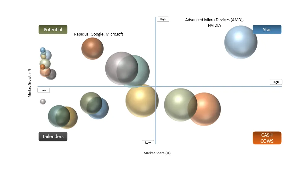
STAR
Advanced Micro Devices (AMD), NVIDIA, Intel, Taiwan Semiconductor Manufacturing Company (TSMC), Samsung Electronics, Broadcom and Marvell Technology form the companies in the Star quadrant owing to their strong market positions along with their leadership role in processors and accelerators featuring chiplets, AI accelerators, advanced packaging and heterogeneous integration.These companies are aggressively bringing in commercialization of new-generation chiplet-based systems on the platforms of AI, HPC, cloud and network applications, while at the same time they are making huge investments in advanced packaging and integration of High Bandwidth Memory (HBM).
POTENTIAL
Rapidus, Google, Microsoft, AWS (Annapurna Labs), MediaTek, Huawei (Hisilicon), SK Hynix and Micron Technology are in the Potential quadrant because of their increased efforts to invest further into custom AI silicon, chiplets, advanced packaging and next-generation semiconductor technologies. Although their product offering in chiplets is not yet at par with that of leading companies, but due to the increasing interest in AI architecture, cloud computing technology, automotive electronics technology, memory chiplet technology and open chiplets, they will definitely have a great potential for growth.
Chiplet Market Dynamics
Driver Impact Analysis
| Driver | Market Growth Impact (%) | Demand Concentration | Impacted Use Case | Strategic Impact |
Rising Demand for AI, High-Performance Computing (HPC) and Data Center Infrastructure | 8.40% | Very High | AI Accelerators, GPUs, HPC Processors, Cloud Servers | Accelerates adoption of chiplet-based architectures to deliver higher compute density, scalability and energy efficiency. |
Growing Adoption of Advanced Packaging and Heterogeneous Integration Technologies | 7.60% | High | Multi-Die Processors, Advanced AI Chips, Networking ASICs | Enables integration of multiple functional dies, improving manufacturing yield, reducing costs and supporting modular semiconductor design. |
Increasing Demand for High-Bandwidth Memory (HBM) Integration | 6.80% | High | AI Training Systems, HPC Clusters, Data Center Accelerators | Drives deployment of chiplet-based processors integrated with HBM through 2.5D and 3D packaging for superior memory bandwidth. |
Rising Investments in Next-Generation Semiconductor Manufacturing and Foundry Capacity | 6.20% | Medium-High | Advanced Logic Devices, Automotive SoCs, AI Infrastructure | Strengthens chiplet ecosystem capabilities by expanding fabrication, advanced packaging and heterogeneous integration capacity worldwide. |
Driver: Rising Demand for AI, High-Performance Computing (HPC) and Hyperscale Data Center Infrastructure
The exponential development in the domains of generative artificial intelligence, HPC and hyperscale cloud is driving the adoption of chiplets in semiconductor technologies. The growing challenges with transistor scaling, manufacturing yields, efficiency and cost associated with monolithic chip design have forced semiconductor manufacturers to implement chiplets in order to combine compute capabilities, memory, I/O capabilities and accelerators in a single package. Chiplet technology provides better performance and scalability advantages, reduced time-to-market and improved cost efficiencies of the devices such as AI accelerators, cloud processors and advanced data center solutions. As a result, growing investment in the infrastructure supporting AI and advanced computing technologies is anticipated to be the main driver for the chiplet market during the forecast period.
Restraint Impact Analysis
| Restraint | Drag on Market Growth (%) | Primary Impact Area | Impacted Use Case | Strategic Impact |
High Design Complexity and Multi-Die Integration Challenges | 5.80% | Chip Design & Integration | AI Processors, HPC Systems, Custom SoCs | Increases development time, validation effort and engineering costs, slowing commercialization of chiplet-based products. |
Limited Advanced Packaging Capacity and High Manufacturing Costs | 5.30% | Semiconductor Manufacturing | AI Accelerators, Data Center Chips | Constrains production volumes and raises overall package costs due to limited availability of advanced packaging technologies. |
Lack of Universal Interoperability Across Proprietary Chiplet Ecosystems | 4.70% | Ecosystem Standardization | Multi-Vendor Chiplet Platforms | Restricts seamless integration of chiplets from different vendors, reducing ecosystem flexibility and scalability. |
Thermal Management and Power Delivery Challenges in Multi-Die Packages | 4.20% | Package Reliability & Performance | AI Servers, HPC Clusters, High-Performance Networking | Increases cooling and power optimization requirements, limiting performance scaling and package reliability in high-density designs. |
Restraint: Limited Advanced Packaging Capacity and High Manufacturing Costs
The large-scale use of architectures using chiplets is hindered due to the scarce presence worldwide of advanced packaging capabilities like CoWoS, SoIC, EMIB, 2.5D and 3D integration. This is because there are only a few foundries and OSATs capable of producing at scale advanced multi-die packages. This fact combined with the large demand for AI accelerators, HPC processors and datacenter processors has created a situation of bottlenecks, extended lead times and increased costs of packaging. All these factors add up to the overall price of semiconductors with chiplets architecture.
Chiplet Market Segmentation Analysis
The global chiplet market is segmented based on the chiplet type, packaging technology, interconnect standard, substrate, integration type, application, end-user, and region.
By Chiplet Type
Compute Chiplets Emerge as the Core of Advanced Semiconductor Design
Compute Chiplets were leading the chiplet market in 2025, as they captured a share of 46.0% in the global market. Compute Chiplets led in the market owing to the growing requirements for AI accelerators, CPUs, GPUs and HPC processors, wherein the multi-die architecture has an edge over traditional monolithic chip in terms of scalability and power optimization. Moreover, the flexibility of integrating the compute chiplets with memory and I/O chiplets along with the efficient utilization of process nodes helped companies to develop more powerful processors for AI and cloud computing faster.
By Application
Artificial Intelligence Accelerates Adoption of Chiplet-Based Architectures
The artificial intelligence (AI) market is forecasted to grow at the highest CAGR of 25.7% during the prediction period. This growth would be supported by the rapid adoption of generative AI technology, large language models (LLM), AI training and AI inferencing solutions and hyperscale data centers expansion. Chiplet-based designs help to increase the compute density, memory bandwidth and power efficiency by connecting several unique dies into a single package. With enterprises and cloud providers making investments in AI infrastructure, chiplet would prove out to be the ideal architecture for future generation AI processors.
Chiplet Market Geographical Penetration
U.S. Chiplet market Landscape
The United States acts as the world’s largest center of chiplet innovation on the back of dominance in AI chips, HPC and semiconductors. The U.S. is being propelled by companies such as AMD, Intel, NVIDIA, Broadcom, Marvell, Apple, Qualcomm and Amazon (Annapurna Labs), which are moving towards modularity and the move from SoCs to chiplets to enhance scalability and performance and increase yield in production. The U.S. is also spearheading the deployment of open chiplet ecosystem models like UCIe, while making huge investments in advanced packaging solutions like Intel’s Foveros and EMIB. Continued high demands from hyperscale cloud providers, generative AI infrastructures, defense applications and advanced networking are pushing for more chiplets to be used. With the backing of the CHIPS and Science Act, increased domestic semiconductor production and close collaborations with top foundry and OSAT companies, the United States is set to be the world’s technological innovator in the chiplet market for the entire forecast period.
Japan Chiplet Market Outlook
Japan is taking shape to be an enabling strategic player in terms of chiplet technology owing to its capabilities in advanced semiconductor material, substrate technology, manufacturing equipment and heterogeneous integration solutions. Japan may not be as prominent in the development of chiplet processors compared to that of the United States and Taiwan; however, companies including Rapidus, Kioxia, Ibiden, Tokyo Electron, SCREEN Holdings and Shin-Etsu Chemical make significant contributions in the entire value chain in chiplet processors. The increasing investment in advanced packaging, chiplet-ready manufacturing processes and next-generation semiconductor manufacturing processes is expected to enhance the relevance of Japan in AI applications, automotive and industrial and high-performance computing. The government's efforts to revive Japanese semiconductor manufacturing industry along with collaboration with international foundry and technology partners is likely to facilitate rapid commercialization of chiplet solutions.
China Chiplet market Trends
China is rapidly developing its chiplets sector with aggressive domestic investment into semiconductor innovations, advanced packaging and heterogeneous integration in order to cut dependence on foreign high-end semiconductors. Companies such as Huawei (HiSilicon), Loongson, Biren Technology, Hygon and Moore Threads have started embracing chiplets-based designs for creating AI accelerators, data center CPUs, network devices and high-performance computing products. The growing capacity for advanced packaging technologies in conjunction with domestic foundries and outsourced semiconductor assembly & test services providers is making China better-equipped to commercialize multi-die semiconductor architectures in spite of technology constraints. Semiconductors-related government initiatives and the rising needs for AI infrastructures, automotive electronics and telecommunications will facilitate further adoption of chiplets in China.
Taiwan chiplet market Overview
The global hub for the manufacturing and advanced packaging in the chiplet industry is Taiwan, thanks to its supremacy in foundry and heterogeneous integration expertise. The presence of TSMC in Taiwan and other technology giants like MediaTek, ASE Technology Holding, SPIL and others makes Taiwan a one-stop-shop offering an end-to-end value chain, including designing, wafer processing, advanced packaging and test services. Technologies including CoWoS, SoIC and advanced 3D packaging have ensured that Taiwan becomes the go-to region for producing AI accelerators, HPC processors and chips used in hyperscale data centers. Collaboration between foundries, OSAT and fabless semiconductor manufacturers globally is further helping in bringing innovations in next-generation chiplets. Owing to its continuous expansion in the area of advanced packaging and increasing applications of chiplets in AI, cloud computing, auto and networking segments, it is evident that Taiwan will remain the top hub for manufacturing and advanced packaging of semiconductors through chiplets.
South Korea chiplet market Analysis
South Korea is becoming a prominent player in the chiplet ecosystem through its expertise and strength in High Bandwidth Memory (HBM), semiconductor manufacturing technology and heterogeneous integration systems. Driven by Samsung Electronics and SK hynix, South Korea plays an integral role as a leading provider of next-generation HBM solutions which are critical for AI accelerators, HPC processors and chiplet-based data center designs. Ongoing research and development efforts in terms of advanced packaging and memory centric designs in 2.5D/3D integration technology make South Korea increasingly competitive in the overall semiconductor ecosystem. The synergy in cooperation among manufacturers of memory chips, foundries, packagers and foreign chip developers for AI applications drives rapid advancement and deployment of high performance multiple die semiconductor devices. Government support and rising demand for AI hardware, cloud services, automotive and network equipment will drive South Korea’s dominance in the chiplet space.
Chiplet market Competitive Landscape
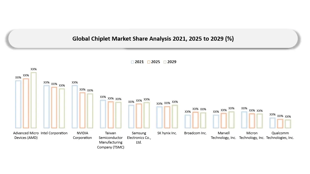
- The industry is slightly concentrated where large firms like AMD, Intel, NVIDIA, TSMC, Samsung Electronics, Broadcom and Marvell use their robust research and development efforts and extensive expertise in semiconductor design along with customer networks to remain at a competitive edge.
- Product differentiation now focuses on having an ecosystem with regards to chiplet, which includes having reuseable chiplet IP, heterogenous integration, die-to-die interconnects, software toolchain and design flexibility instead of having just process nodes.
- Packaging and manufacturing have become strategic competitive assets, with businesses gaining secure access to leading-edge foundries, OSATs and advanced packaging techniques in order to promote commercialization and scalability.
- Competition is extending to nontraditional players in the semiconductor market, in that hyperscale cloud players and custom silicon producers are rolling out more and more application-specific chiplets for AI, cloud computing, networking and edge computing applications.
- Through acquisitions, collaboration in ecosystems and the adoption of industrial standards, competitive dynamics are being redefined, such that companies are able to extend their technology offerings and cycles of innovation.
Chiplet Leading industry players
- Advanced Micro Devices (AMD) (United States)
- Intel Corporation (United States)
- NVIDIA Corporation (United States)
- Taiwan Semiconductor Manufacturing Company (TSMC) (Taiwan)
- Samsung Electronics Co., Ltd. (South Korea)
- SK hynix Inc. (South Korea)
- Micron Technology, Inc. (United States)
- Broadcom Inc. (United States)
- Marvell Technology, Inc. (United States)
- Qualcomm Technologies, Inc. (United States)
- MediaTek Inc. (Taiwan)
- Apple Inc. (United States)
- Google LLC (United States)
- Microsoft Corporation (United States)
- GlobalFoundries Inc. (United States)
- Amazon Web Services (Annapurna Labs) (United States)
- Huawei Technologies Co., Ltd. (HiSilicon) (China)
- IBM Corporation (United States)
- Rapidus Corporation (Japan)
- Bosch Semiconductor (Germany)
chiplet market Major Pain Points
- Insufficient interoperability among chiplets supplied by multiple vendors is holding back the complete emergence of open multi-vendor chiplet ecosystem in spite of the fact that semiconductor industry has already moved on to using the UCIe standardization platform.
- There are limitations in the capacity of advanced packaging technology such as CoWoS, 2.5D and 3D integration platforms causing manufacturing difficulties of AI and HPC processors using chiplets.
- Complexities associated with design, verification, validation and lifecycle management of multi-die products increase cost and increase the time-to-market.
- It becomes very difficult to manage thermal dissipation, power distribution and signal integrity as compute, memory and IO chiplets get packaged together within a dense packaging technology.
- Chiplet architecture is still heavily dependent on very few foundries, OSATs and HBM vendors, which increases supply chain risk and decreases manufacturing options.
Chiplet market Recent Developments
- May 2026: NVIDIA Corporation increased manufacturing speed of its AI platform called Rubin with the use of future-proof chiplet architectures and technologies along with HBM4 in the AI computing system.
- July 2026: Intel Corporation introduced EMIB-T (Embedded Multi-Die Interconnect Bridge Technology) that allowed to deliver better power and interconnect performance for multi-die packages combining processors, graphics processors, HBM and I/O dies.
- September 2025: Micron Technology started mass production of its 36GB 12-High HBM3E memory suited for heterogeneous AI systems, effectively bolstering its next-generation chiplet-centered accelerator platforms.
- May 2026: NVIDIA Corporation enhanced production capabilities for its Rubin AI platform, integrating cutting-edge chiplet architecture and packaging technology with HBM4 features for the hyperscale AI infrastructure.
- July 2026: Intel Corporation launched EMIB-T (Embedded Multi-Die Interconnect Bridge Technology), which provides better power delivery and improved interconnect performance for single big multi-chiplet packages that combine CPUs, GPUs, HBM and I/O dies.
Analyst View / Opinion on chiplet market
- Chiplets are gaining traction within the industry as the chosen method of continuing the scaling of performance beyond Moore's Law constraints and allowing for modular and cost-effective semiconductor architectures.
- With the increasing pace of commercial deployment of AI accelerators and data center processors, we can expect that chiplet-based architectures will be used widely in future high-performance computing solutions.
- Adoption of open interconnects like UCIe standard will spur multi-vendor systems of chiplets, ensuring interoperability, reuse and quick development of semiconductor products.
- New packaging techniques like 2.5D packaging, 3D packaging, Fan-Out packaging and SiP are gaining more significance and acting as competitive advantage as companies look to gain more leverage from packaging rather than just process nodes.
- Companies that have a great ability to leverage chiplet design, advanced packaging techniques, foundries as well as ecosystem are sure to have a sustained competitive advantage due to the shift towards heterogenous integration.
chiplet market Target Audience
| INDUSTRY | WHO SHOULD BUY THIS REPORT? | REASON TO BUY THIS REPORT |
| Semiconductor Manufacturing | Integrated Device Manufacturers (IDMs), Foundries, Fabless Semiconductor Companies | Evaluate chiplet adoption trends, technology roadmaps and competitive positioning. |
| Advanced Packaging & OSAT | OSAT Providers, Advanced Packaging Companies | Assess demand for 2.5D/3D packaging, heterogeneous integration and capacity expansion opportunities. |
| Electronic Design Automation (EDA) | EDA Software Vendors, IP Providers | Understand evolving chiplet design requirements, interoperability standards and ecosystem developments. |
| Cloud Computing & Data Centers | Hyperscale Cloud Providers, Data Center Operators | Identify chiplet-based processor adoption trends for AI, HPC and cloud infrastructure investments. |
| Artificial Intelligence | AI Hardware Developers, Accelerator Manufacturers | Evaluate demand for chiplet-enabled AI processors, HBM integration and next-generation compute platforms. |
| Telecommunications & Networking | Telecom Equipment Manufacturers, Networking Solution Providers | Analyze opportunities for chiplet adoption in 5G, Open RAN, networking ASICs and edge infrastructure. |
| Automotive | Automotive OEMs, Tier-1 Suppliers, Autonomous Driving Technology Providers | Assess the role of chiplets in ADAS, autonomous vehicles, digital cockpits and high-performance automotive computing. |
| Consumer Electronics | Smartphone, PC, Gaming Console and AR/VR Device Manufacturers | Track chiplet integration strategies for next-generation consumer electronic devices. |
| Government & Research | Government Agencies, National Semiconductor Programs, Research Institutions | Support semiconductor policy development, R&D planning and domestic chip manufacturing initiatives. |
| Investment & Financial Services | Venture Capital Firms, Private Equity Firms, Institutional Investors, Strategy Consultants | Evaluate market growth potential, investment opportunities, competitive landscape and emerging technology trends. |
Why Choose DATAM?
- Data-Driven insights: Dive into detailed analyses with granular insights such as pricing, market shares and value chain evaluations, enriched by interviews with industry leaders and disruptors.
- Post-Purchase Support and Expert Analyst Consultations: As a valued client, gain direct access to our expert analysts for personalized advice and strategic guidance, tailored to your specific needs and challenges.
- White Papers and Case Studies: Benefit quarterly from our in-depth studies related to your purchased titles, tailored to refine your operational and marketing strategies for maximum impact.
- Annual Updates on Purchased Reports: As an existing customer, enjoy the privilege of annual updates to your reports, ensuring you stay abreast of the latest market insights and technological advancements. Terms and conditions apply.
- Specialized Focus on Emerging Markets: DataM differentiates itself by delivering in-depth, specialized insights specifically for emerging markets, rather than offering generalized geographic overviews. The approach equips our clients with a nuanced understanding and actionable intelligence that are essential for navigating and succeeding in high-growth regions.
- Value of DataM Reports: Our reports offer specialized insights tailored to the latest trends and specific business inquiries. The personalized approach provides a deeper, strategic perspective, ensuring you receive the precise information necessary to make informed decisions. The insights complement and go beyond what is typically available in generic databases.
What DATAM Uniquely Provides
- Forecast analysis for chiplet by type, packaging technologies, interconnect technologies, applications, end-user types and regional markets up to 2035.
- Competitive intelligence analysis with details on prominent chiplet suppliers, foundries, OSAT companies, technology alliances, product launches and investments.
- Technology perspectives on the heterogeneous integration, UCIe implementations, 2.5D/3D packaging technologies, HBM integration and multichip semiconductor architecture trends that will define future generation chip designs.
- Ecosystems and supply chain analysis identifying how IDMs, fabless companies, fabs, OSAT vendors and equipment manufacturers fit into the global chiplet supply chain.
- Actionable strategies that identify new market opportunities and growth investments within this dynamic semiconductor technology ecosystem.