Advanced Packaging Substrate Market Size and Overview
The global advanced packaging substrate market reached US$ 16.92 billion in 2025 and is expected to reach US$ 33.3 billion by 2035, growing with a CAGR of 7.0% during the forecast period 2026-2035.
One of the major factors that contribute to the advancement of the market for advanced packaging substrates is the rapid growth of technologies like artificial intelligence (AI), high-performance computing (HPC) and semiconductor packaging. The technologies have increased the demand for larger substrates, higher I/O density, finer interconnections and better thermal and power management. According to SEMI, there was an increase of 20.8% in the sales of semiconductor packaging and assembly equipment during the year 2025 and it is expected that it will reach US$6.7 billion in 2026. It shows that continuous investments are being made in the field of advanced packaging for artificial intelligence and HBM devices. Moreover, as more and more chiplets and HBM technologies are being used, the demand for advanced types of substrates like FC-BGA, FC-CSP, SiP and MCM has also increased tremendously and investment in new advanced equipment has been accelerated.
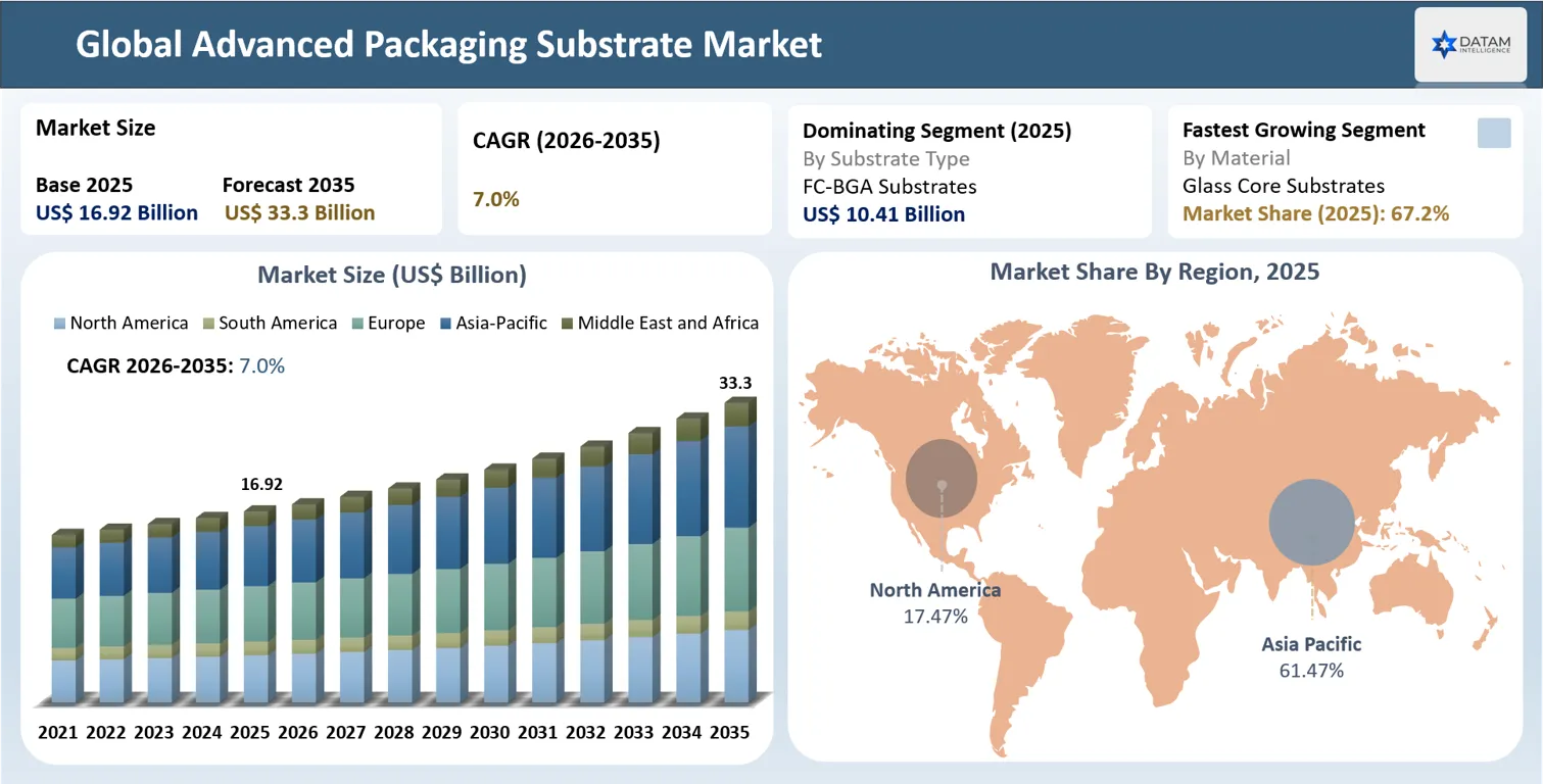
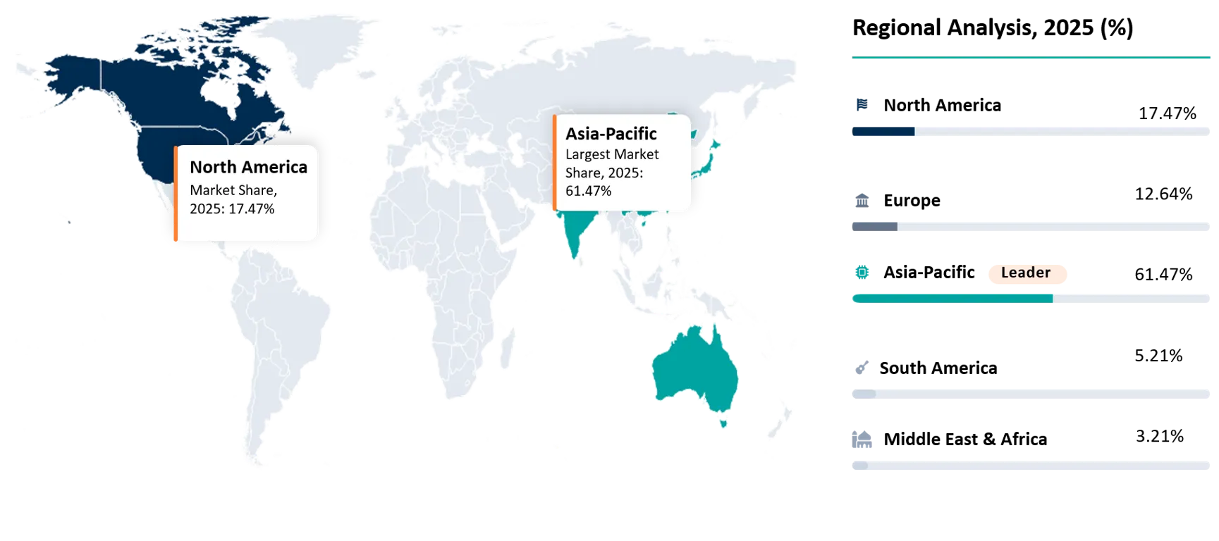
Asia-Pacific is a major region for advanced packaging, given its semiconductor and substrate manufacturing industry in countries like Taiwan, Japan, South Korea and China. Glass core substrates are becoming important at the forefront of technology due to their stability, rigidity and ability to provide a highly dense interconnection that can solve the problems associated with scaling in large AI and HPC packages. As per SEMI, the amount of opportunity presented by glass core substrates may amount to around US$13 billion by 2040, which thus also opens doors for investment in various sectors, including glass materials, TGV processing, metallization, inspection and advanced substrate manufacturing.
Advanced Packaging Substrate Market Key Takeaways
- FC-BGA (Flip Chip Ball Grid Array) Substrates held a dominant position in the global advanced packaging substrate market in 2025, commanding an approximate 61.5% market share due to the rising popularity of AI accelerators, HPC processors, server CPUs, GPUs and networking devices.
- Glass core substrates are forecasted to be the most rapidly growing material type, registering an approximate 67.2% CAGR from 2028 to 2040, as reported by SEMI, owing to the widespread use of Glass Core substrates in AI, HPC and large format advanced packaging applications.
- The Asia Pacific is the leader in the global advanced packaging substrate market, occupying 61.47% market share in 2025 due to the presence of many IC substrates, semiconductor foundries, OSATs and advanced packaging players in the region including Taiwan, South Korea, Japan and China.
- The fast deployment of 2.5D and 3D packaging technology increases the complexity of the substrate technology, where the need for chiplet, HBM, larger packages and higher I/Os requires fine line/space geometry, higher layers, signal integrity and reduced warpage.
- Growing demand for semiconductor chips for AI accelerator and data center applications compels substrate companies to shift to large format FC-BGA, advanced ABF substrate material, SAP/mSAP process and Glass Core substrates, whereas development in TGV process, metallization and yield improvement can help in expanding capacity in the future.
Advanced Packaging Substrate Industry Trends and Strategic Insights
- The demand for larger, higher-layer-count, fine-line package substrates is being driven by the combination of AI and HPC, with a need for high density FC-BGA substrates, improved warpage and enhanced power/signal routability becoming essential.
- Chiplet-based 2.5D/3D technologies are making substrates more complicated with the need for more advanced interconnect capabilities including bridge integration, smaller geometry and enhanced routability.
- Materials and capacity issues are emerging as strategic chokepoints, especially for AI-based ABF substrates, because larger packages use significantly more materials and it is difficult to scale-up and qualify additional capacity.
- Strategic investments are being made throughout the substrate value chain, where chipmakers and material suppliers are working on glass-based materials development, packaging collaborations and regional manufacturing capacity.
Advanced Packaging Substrate Market Scope
| Metrics | Details | |
| 2025 Market Size | US$ 16.92 Billion | |
| 2035 Projected Market Size | US$ 33.3 Billion | |
| CAGR (2026-2035) | 7.0% | |
| Largest Market | Asia-Pacific | |
| Fastest Growing Market | Asia-Pacific | |
| By Substrate Type | FC-BGA (Flip-Chip Ball Grid Array) Substrates, FC-CSP (Flip-Chip Chip Scale Package) Substrates, SiP (System-in-Package) Substrates, Multi-Chip Module (MCM) Substrates and Others | |
| By Material | Organic Substrates (ABF-Based, BT Resin-Based), Ceramic Substrates, Glass Substrates and Others | |
| By Substrate Structure | Core Substrates and Coreless Substrates | |
| By Manufacturing Technology | Subtractive Process, Semi-Additive Process (SAP), Modified Semi, Additive Process (mSAP) and Others | |
| By Packaging Architecture | 2D Packaging, 2.5D Packaging and 3D Packaging | |
| By Application | High-Performance Computing (HPC) & AI, Consumer Electronics, Automotive Electronics, Telecommunications & Networking, Industrial, Healthcare, Aerospace & Defense and Others | |
| By Region | North America | U.S., Canada, Mexico |
| Europe | Germany, UK, Russia, France, Spain, Italy, Poland | |
| Asia-Pacific | China, India, Japan, Australia, South Korea, Indonesia, Malaysia, Singapore, Vietnam, Thailand, Philippines, Taiwan | |
| South America | Brazil, Argentina | |
| Middle East and Africa | UAE, Saudi Arabia, South Africa, Israel, Turkiye, Nigeria | |
| Report Insights Covered | Competitive Landscape Analysis, Company Profile Analysis, Market Size, Share, Growth | |
Why does this report matter in 2026?
In 2026, advanced packaging substrates have become the key limiting factor in scaling up AI accelerators, high-performance computing processors, and data center semiconductors. The growing package sizes, increasing I/Os, smaller circuits and growing popularity of chiplet-based 2.5D and 3D solutions have created an increased demand for advanced substrates such as FC-BGA, FC-CSP, SiP and MCM substrates. This means that information on substrate capacities, technology roadmaps, material availability and manufacturing yield rates have become increasingly crucial for semiconductor companies.
The report has great significance because the industry is transitioning from traditional organic substrates to future generation glass core substrates that have inherent advantages in dimensionally stable, warpage-controlled and large-package integration capability. Through substrate material evaluation, manufacturing technology evaluation, packaging architecture evaluation, regional capacity assessment, application demand assessment and competitive strategy analysis, this report assists interested parties in identifying areas where substrate constraints can arise, technologies reaching maturity and investment opportunities.
Advanced Packaging Substrate Market White Space & Investment Opportunities
- AI/HPC FC-BGA capacity expansion: There is an investment opportunity in the development of large-format and high-layer-count and fine-line FC-BGAs, due to the need for higher I/O density in AI accelerators, GPUs and processors used in data centers.
- Glass Core Substrates commercialization: Glass Core Substrates are one of the key technology gaps for future AI and HPC packaging, especially in technologies such as TGV fabrication, metallization, fine-line patterning, warpage management and large-format substrates.
- Chiplet and 2.5D/3D substrate platforms: There is an investment opportunity in substrate technologies that support multi-die packaging, high-bandwidth memory interface, high-density interconnects and power delivery technologies as heterogenous integration becomes more complicated.
- Advanced substrate equipment and process ecosystem: White-space opportunities go well beyond substrate suppliers into TGV drilling, laser processing, copper metallization, CMP, redistribution layer (RDL), inspection and yield enhancement technologies needed to realize next-gen glass and high-density substrates.
- Regionalized advanced packaging capacity: With new manufacturing investments being made in Asia-Pacific, North America and other regions of semiconductor production, there is an opportunity to produce substrates and materials locally, while having alternative second sources of capacity.
Advanced Packaging Substrate Future Market Transformation
As the complexity of 2.5D and 3D systems increases, demands on substrates will increasingly focus on I/O density, power delivery, signal integrity, thermal management and warpage. Meanwhile, Glass Core Substrates are progressing towards commercialization due to their stiffness and dimensional stability, as well as compatibility with large area packages, while manufacturing yield and glass/resin interface reliability are still key issues in this process.
The competition in the future will not only be limited to the substrate capacity but will include material innovation, glass-core processing, sophisticated interconnection technology, chiplet-enabled substrate technology and intelligent manufacturing and yield enhancement technology. The differentiation among competitors in the future will largely depend on the capability to incorporate substrates within next-generation packaging technology in an economic manner. The shift is expected to provide opportunities to existing FC-BGA and IC substrate providers and new players in Glass Core Substrates.
Advanced Packaging Substrate Market Buyer Decision-Making Criteria
Buyers in the advanced packaging substrate market evaluate vendors according to their capacity to provide high density, dimensionally stable and dependable substrates capable of meeting the needs of semiconductor packages from an electrical, thermal, mechanical and processing standpoint. The buying decision process is especially impacted by the performance of substrates used in the packaging of AI/HPC processors, chiplets, 2.5D/3D technology nodes and larger-sized FC-BGA. Buyers also consider TGV capability, dimensional stability, matching CTE, glass handling and market-readiness when assessing Glass Core Substrates.
Major Buyer Decision-Making Criteria
- Fine-Line & High-Density Interconnect Capability
- Warpage & Dimensional Stability
- Electrical & Signal Integrity Performance
- Thermal Management & CTE Matching
- Substrate Reliability & Qualification
- Manufacturing Yield & Process Consistency
- Large-Format Substrate Capability
- SAP/mSAP Manufacturing Expertise
- Glass Core & TGV Processing Capability
- Production Capacity & Scalability
- Material Availability & Supply Security
- Cost per Substrate & Total Package Economics
- Technology Roadmap & Innovation Capability
- Automotive/Data-Center Qualification Track Record
- Global Manufacturing & Customer Support Footprint
Advanced Packaging Substrate Market Economic & Investment Analysis
The advanced packaging substrates market will be going through a capital-intensive growth phase due to the need for AI accelerators, HPC processors, HBM-equipped packages and chiplets architecture that need bigger, finer line and denser substrates. By 2026, capacity shortages of advanced ABF substrates are making the development of new capacities, long-term customer relationships and yield capability more important. Therefore, major players in substrates are allocating a lot of capital towards capacity for AI/HPC FC-BGA and investors are starting to take into account substrate shortages in the overall AI semiconductor supply chain.
Investment is also becoming more prevalent in Glass Core Substrates and the infrastructure that surrounds them, such as the process of TGV, metallization, testing and inspection, materials and specific equipment. Glass substrates have become an area of investment due to their possibilities for enhanced dimensional stability, smaller interconnect density and increased AI/HPC package sizes. An example of the magnitude and geographical spread of emerging investment is the suggested US$3.3 billion Intel–3D Glass Solutions glass-core substrate plant in Odisha, India.
Advanced Packaging Substrate Investment Trends in the Market
- AI-driven FC-BGA capacity expansion: Investments are becoming increasingly geared towards manufacturing large FC-BGA substrates with many layers and thin lines because AI processors use much more substrate capacity and ABF substrate is experiencing supply shortage issues.
- Glass Core Substrate commercialization: Investments are moving towards Glass Core Substrates where companies invest in TGV, metallization, inspection and large panel manufacturing for meeting future requirements of AI and HPC packages.
- Regionalization of substrate manufacturing: Diversification in the semiconductor supply chain is leading to investments in advanced substrates beyond the usual locations of production in East Asia with large-scale projects in India and North America for packaging capabilities.
- Investment in advanced process and yield technologies: Investment is being made in fine line lithography, SAP/mSAP, inspection, TGV process, metallization and yield enhancement equipment since the level of manufacturing difficulty is now considered an important factor for next generation substrates.
- Strategic capacity commitments for AI supply chains: Semiconductor companies and hyperscalers involved in AI are attaching more significance to having the required capacity and suppliers in order to overcome the potential problem of shortage of substrates in the upcoming packaging expansion cycle.
Strategic Indicators For the Advanced Packaging Substrate Market
High Regulation Impact
The advanced packaging substrate market is encountering growing demands linked to procedures and standards that include chemical materials, sustainability compliance, traceability, safety in manufacturing and substrate durability. All regulations impact ABF, BT resin, ceramic and even newly introduced Glass Core Substrates, thus being relevant in the delivery of dimensions, temperature, TGV and measurement requirements for obtaining qualification and making commercial use of such materials. Programs for advanced packaging funded by the government are also focused on supporting the locally produced goods over the imported ones, as well as technology qualification issues and therefore compliance must be taken into consideration when planning future capacity expansion or supplier selection.
High Investment Activity
Investment is very high in the advanced packaging substrate market due to the increased demand for AI and HPC resulting in capacity investments in large size FC-BGA and high density substrates. Substrate producers in 2026 will be investing significant funds in building additional capacity in substrates, Glass core substrates, TGV processing, advanced metallization and even special manufacturing equipment. Initiatives taken by companies like AT&S, Ibiden, Samsung Electro-Mechanics and glass core projects related to Intel illustrate the increased investment in conventional and next generation substrates.
Supply Chain Disruption
In the advanced packaging substrate market, there is growing supply chain tension in the market due to the need for increased size and number of layers in FC-BGA substrates that are necessary for AI and HPC processors, which results in increased demand for ABF, T-Glass, CCLs and substrate production capabilities. The lack of availability of raw materials upstream, small number of suppliers, long qualifying periods and years needed to build out advanced substrate facilities can create bottlenecks even when semiconductor wafer capacity is available. The ABF substrate availability is seen as one of the critical challenges in the AI semiconductor supply chain in 2026, which leads to long-term capacity commitments by customers.
Pricing Volatility
The pricing fluctuation in the advanced packaging substrate market will be caused by AI/HPC-driven demand, ABF supply tightness, rising T-glass and copper prices and growing substrate complexities.ABF substrate prices have risen between 5-10% in 2026 compared to Q2 prices, with some spot prices having risen by more than 30%. Industry sources suggest that prices can increase by 3-5% every quarter within the first half of 2026.In addition to the above, Ajinomoto has announced a price hike in ABF build-up film by 30%, which will take effect from Q3 2026, increasing cost pressure across substrate manufacturers.
Procurement Pressure
Pressure on Procurement in the advanced packaging substrate market is growing because of the need for increased supply of advanced packaging substrates required by AI accelerators, HPC chips and chiplet packages, leading to the limited availability of ABF material, copper foil, glass reinforcement material and manufacturing capacity. In order to mitigate allocation risk and lengthy qualification process, buyers are focusing more on securing capacity, material stock and multi-sourcing from qualified suppliers. Glass Core Substrates, in turn, present an additional challenge for procurement since qualified materials and technologies, including glass material, TGV technology, metallization and equipment are needed prior to scaling up the production.
New Technology Adoption
The adoption of new technology in the advanced packaging substrate market is gaining momentum in terms of fine-line SAP/mSAP technology, large-size FC-BGA substrates, architectures compatible with Chiplets in 2.5D/3D and Glass Core Substrates. High I/O density, power delivery, dimensional control and lower warpage needs of the AI and HPC packaging drives the need for advanced material, TGV glass interconnection, metallization and automation in the inspection of substrates. Adoption of Glass Core Substrates becomes significant as the manufacturers look for scaling of their solution for the next generation of packages where the organic substrate faces issues of dimension and warpage.
Regional Expansion Opportunity
The advanced packaging substrate market is experiencing a growth in regional expansion opportunities, as economies of semiconductor ecosystems are starting to localize advanced packaging capacity and reduce reliance on concentrated Asian supply chains. The most significant manufacturing centers are in Asia-Pacific, including Taiwan, South Korea, Japan and China, while both India and the United States have started to emerge as attractive locations for new substrate and advanced packaging investments. There are excellent prospects in the area of FC-BGA production (AI/HPC), substrate manufacturing using ABF technology and latest-generation glass substrates. These developments can count on the government’s support, proximity to semiconductor fabs and OSAT companies and growing demand for locally-produced substrates.
Government Policy Support
Government initiatives are contributing positively to the advance of the advanced packaging substrate market by providing subsidies for semiconductor production, funding for advanced packaging R&D and domestic supply chain initiatives. Programs in the U.S., India, Japan, South Korea, Taiwan and Europe are promoting local manufacturing of IC substrates, ABF-based materials, advanced packaging solutions and newer Glass Core Substrates, along with providing support for investments in high-density packaging, chiplet technology and new substrate production. Such initiatives bring down the barriers for investments, increase local manufacturing capability and boost supply chain security for AI, HPC, automotive, as well as other semiconductor uses.
Pricing Intelligence
In the advanced packaging substrate market, pricing intelligence is increasingly governed by substrate size, layer count, line/space design, materials used and package complexity instead of being dictated only by the volume of products. Current projections indicate that average sales price per unit of ABF substrate has increased from US$65 in 2024 to US$82 in 2025, whereas high-end AI or HPC substrates are responsible for having even higher prices due to the production of bigger packages, more layers used and stricter process conditions. Moreover, material expenses account for more than 50% of the advanced packaging expenses and IC substrate one itself can cost at least half of the total expenses for FC-BGA packaging, meaning that efficiency in terms of material usage, production yields and substrate design are crucial for pricing strategies and profit margins of suppliers.
| HS Code | Reporter | Trade Flow | 2025 Trade Value | Interpretation |
| 8542.9 | Taiwan | Export | $14.53 Billion | Indicates Taiwan's significant role in the global semiconductor manufacturing, component and advanced packaging supply chain ecosystem. |
| 8542.9 | China | Import | $18.91 Billion | Reflects the scale of China's semiconductor and electronics manufacturing, assembly and component processing ecosystem. |
| 8542.9 | South Korea | Export | $9.24 Billion | Underscores South Korea's established position within the global semiconductor component and integrated-circuit supply chain. |
| 8542.9 | United States | Import | $11.67 Billion | Highlights substantial demand from the U.S. semiconductor, computing and advanced electronics ecosystem. |
AI Impact Analysis of the Advanced Packaging Substrate Market
AI systems are becoming one of the key demand drivers for advanced packaging substrates because AI accelerators, GPUs, CPUs, network processors and systems with HBM need bigger package sizes, more I/Os, smaller interconnects and improved power delivery. The trend towards using chiplets and 2.5D/3D designs is driving increased demand for high layer count FC-BGA and ABF substrates and bigger AI packages are leading to higher demands in areas such as warpage, thermal management, signal integrity and manufacturing yields.
In addition, AI is also speeding up changeover in technology and investments taking place in the substrate eco-system, especially with regards to Glass Core Substrates. The increase in package size makes glass a candidate for dimensional stability and lower CTE. With glass, the potential for precise structures in AI/HPC packages is possible in the future. In this regard, companies have started making investments in glass core research and development, thin glass via etch processing, advanced metallization and manufacturing capabilities.
Disruption Analysis of Advanced Packaging Substrate Market
The advanced packaging substrate market is currently experiencing disruptions to its supply chain due to the increasing complexity and sizes of both AI packages and high-performance computing (HPC) packages. This has led to a significant increase in demand for high-level ABF substrates, large-scale FC-BGA designs, low-CTE T-glass and advanced manufacturing technologies. As a result, there is a current supply gap of approximately 10% for ABF substrates as of 2026 and new production capacities would require time to be tested and approved. There is thus an increase in risks of product allocation and lead times of procurement and importance of having effective agreements for long-term supply of substrates.
Disruption is also driving the change to Glass Core Substrates due to the issues that arise with conventional organic substrates in terms of warpage, dimensional stability and scaling of large packages. Nevertheless, glass brings about a set of its own manufacturing and reliability issues, such as TGVs, metallization, CTE, edge cracks and SeWaRe defects. Therefore, disruption is transforming not only substrate sourcing but also material selection, manufacturing processes, supplier capabilities and investments.
Advanced Packaging Substrate Market BCG Matrix: Company Evaluation
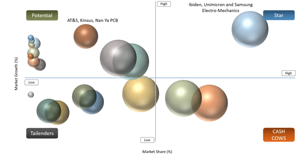
STAR
Ibiden, Unimicron and Samsung Electro-Mechanics are labeled as Stars, as they leverage their strength in both strong exposure to the demand for AI/HPC substrates that grow rapidly and their capability in producing high-end FC-BGA and advanced semiconductor package substrates. The investments in substrates of large format, high layer counts and next-generation further reinforce their advantage in capturing the growing demand.
POTENTIAL
Potential firms like AT&S, Kinsus, Nan Ya PCB and Daeduck Electronics stand out in this case because of their capability to grow stronger in the industry with increased AI/HPC use and evolving advanced packaging needs. These firms have the opportunity to grow due to their competence in IC substrates and FC-BGA technology, although further investments in HDI, substrate sizes, production and Glass Core Substrates will benefit them in the future.
Advanced Packaging Substrate Market Dynamics
Driver Impact Analysis
| Driver | Market Growth Impact (%) | Demand Concentration | Impacted Use Case | Strategic Impact |
Rising Demand for AI, HPC & Data Center Processors | 32% | High | AI accelerators, GPUs, CPUs & servers | Drives demand for high-density FC-BGA and next-generation substrates |
Growing Adoption of Advanced Packaging & Heterogeneous Integration | 27% | High | Chiplets, 2.5D/3D ICs & SiP | Increases substrate complexity, interconnect density and value per package |
Expansion of 5G & High-Speed Networking Infrastructure | 18% | Medium-High | Network switches, routers & telecom equipment | Supports demand for high-frequency and high-performance package substrates |
Increasing Semiconductor Content in Automotive Electronics | 13% | Medium | ADAS, EVs & domain controllers | Expands demand for reliable, thermally efficient and high-density substrates |
Driver: Rising AI & HPC Semiconductor Demand
The rise of AI accelerators, GPUs, CPUs in servers, processors with high-bandwidth memory and AI networking chips has brought about a considerable increase in the need for advanced packaging substrates. These devices necessitate extended package footprints as well as higher data I/O density and power requirements, which increases the need for high-level FC-BGA and ABF-based substrates. The revenue from ABF substrate-for-GPU applications from AI and data center GPUs in 2025 accounted for 63.17% while revenue from advanced FC-BGA substrates for 2.5D and chiplet GPUs reached 56.88%, indicating the high concentration of demand for advanced substrates in AI-based packaging solutions.
Restraint Impact Analysis
| Restraint | Drag on Market Growth (%) | Primary Impact Area | Impacted Use Case | Strategic Impact |
High Manufacturing Complexity and Capital Intensity | 30% | Production capacity & yield | Advanced FC-BGA, 2.5D/3D packaging | Raises entry barriers and slows capacity expansion |
Limited Availability of Advanced Substrate Materials | 25% | Raw material supply chain | ABF-based and high-density organic substrates | Creates supply bottlenecks and increases procurement risks |
High Defect Rates and Yield Challenges at Fine-Line Geometries | 20% | Manufacturing yield | AI/HPC and high-density chiplet packages | Increases production costs and limits scalable manufacturing |
Long Technology Qualification and Customer Certification Cycles | 15% | Product commercialization | Automotive, data center & advanced semiconductor applications | Delays adoption of new substrate technologies |
Restraint: High Manufacturing Complexity and Capital Intensity
Advanced packaging substrate market faces restrictions due to expensive investment cost and complicated production processes for large-sized FC-BGA, fine line SAP/mSAP and high-layer-count substrates. In the case of AI/HPC packages, more challenging line/space, higher layer count, bigger substrate body size and warpage/yield control need substantial investments in high-end lithography, laser drill, plating, inspection and process control equipment. Consequently, prolonged qualification period, yield issues and the high cost of increasing production capacity make production ramp-up difficult for small companies to compete in high-end substrate applications.
Advanced Packaging Substrate Market Segment Analysis
The global advanced packaging substrate market is segmented based on the substrate type, material, substrate structure, manufacturing technology, packaging architecture, application and region.
By Substrate Type
FC-BGA Substrates lead the market as AI and HPC packages demand higher I/O density
In 2025, the market for FC-BGA substrates held a major share of 61.5% in the advanced packaging substrate market, owing to their wide application in AI accelerators, GPUs, server CPUs, HPC processors and high-speed networking components. Growing trends towards larger packages, increased numbers of I/Os and stringent power and signal routing needs are creating a demand for bigger multilayer FC-BGA substrates with small line/space geometry.
By Material
Glass Core Substrates represent the fastest-growing material opportunity as large AI packages scale
Glass core substrates are expected to be the fastest growing materials segment. Its ability to offer high dimensional stability, minimal warping, integration into larger format packaging and the formation of high-density interconnects makes them more applicable to next-gen AI and HPC packages, while TGV and metallization technologies have been advancing their move towards commercial readiness.
Advanced Packaging Substrate Market Geographical Penetration
Taiwan Advanced Packaging Substrate Market Analysis
Taiwan has become a leading center for substrate development due to the presence of a well-integrated ecosystem consisting of IC substrate producers, semiconductor foundries, OSATs, suppliers of materials and advanced packaging customers. Unimicron, Nan Ya PCB and Kinsus are highly exposed to ABF and FC-BGA substrates, while the rapidly increasing demand for AI servers and HPC is increasing substrate usage, large size packages and capacity investments. In 2026, the suppliers of substrates from Taiwan are receiving a benefit from high AI demand, as the companies like Unimicron, Nan Ya PCB and Kinsus saw very strong year-over-year revenues in July and according to Unimicron, AI-related products made up more than 60% of revenue in the first half of 2026. Thus, Taiwan has the opportunity to capture the growth in AI/HPC substrates, advanced ABF technology and Glass Core Substrates, despite the fact that there are several constraints.
South Korea Advanced Packaging Substrate Market Projection
The advanced packaging substrate market in South Korea is poised for considerable growth as AI processors, server processors, HBM-enabled technologies and supercomputing create a requirement for large, multi-layered FG-BGA substrates. The advanced IC substrates market in South Korea was valued at approximately U.S. $ 1.4 billion in 2025 and is forecast to hit around $3.6 billion by 2035, achieving a CAGR of approximately 9.75 %. Samsung Electro-Mechanics is stepping up the provision of high-value FCBGA solutions to AI processors and server processors; South Korean companies are also increasing their investments in large substrates and advanced technologies. In other words, growth in AI-enabled substrate demand, local production expansion and an increasing uptake of advanced packaging technologies will create opportunities in the market, particularly for Glass Core Substrates.
Japan Advanced Packaging Substrate Market Outlook
Japan is projected to continue being a strategic high-value market for advanced packaging substrates, backed up by the country’s excellence in ABF material, high-performance IC package substrates, advanced manufacturing technology and semiconductor materials. The driving demand would come from AI GPUs, AI ASICs, HPC processors, networking ICs and increasingly bigger 2.5D/3D packages, which have seen Japanese players making huge investments in next-generation capacity. Ibiden plans to invest in the neighborhood of JPY 500 billion (about US$3.1-3.3 billion) through FY2028 in high-performance IC package substrates, including capacity allocation for AI ASIC and AI GPU applications, with mass production scheduled in FY2027. Japan is also gaining importance as a development hub for Glass Core Substrates, as substrate requirements evolve towards larger size, more layers, finer geometry and better warpage control.
China Advanced Packaging Substrate Market Trends
China's advanced packaging substrate market is shifting towards higher-end IC substrate localization based on the advancements in AI computing, HPC, 5G and advanced packaging. Local producers are speeding up their R&D efforts in FC-BGA, ABF substrate and high-density packaging solutions, while investments in advanced packaging, substrate materials and equipment are being made in increasing numbers. China's IC packaging substrate market is expected to grow from an estimated $3.15 billion in 2025 to $5.63 billion by 2030, achieving a CAGR of 12.3%, thanks to AI demand and domestic substitution. Meanwhile, Glass Core Substrates technology is becoming strategic, with BOE initiating production of glass core substrates for large-scale computing chips and Chinese companies making more investments into TGV, metallization and other glass processing.
U.S. Advanced Packaging Substrate Market Landscape
The U.S. advanced packaging substrate market is being formed as a critical capability in domestic semiconductors on the back of increasing AI/HPC requirements, investments into advanced packaging and supply chain localization efforts backed by government. Intel is moving forward with development of 2.5D/3D packaging capabilities, chiplet technologies, EMIB and Foveros packaging for future AI processors, whereas advanced packaging programs on the federal level facilitate development of domestic capabilities in terms of R&D and manufacturing of organic substrates, glass substrates and others. Furthermore, the U.S. is becoming an important hub for Glass Core Substrates, with firms like Absolics working on commercialization and investments increasing in glass-based packaging technologies. Overall, the market holds potential in AI/HPC FC-BGA substrates, advanced interposers, Glass Core Substrates, TGV technology and localized substrate manufacturing, yet the capabilities are less developed compared to ecosystems in Taiwan, South Korea and Japan.
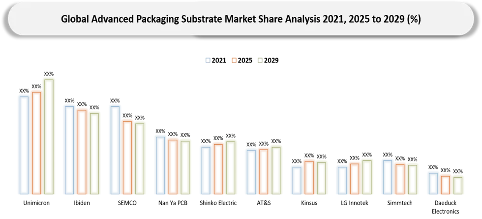
Advanced Packaging Substrate Market Competitive Landscape
- The top-tier players are focusing on their FC-BGA capabilities for AI/HPC applications. Companies like Ibiden, Unimicron and Samsung Electro-Mechanics are adding to their capabilities by supporting larger package sizes, higher layer counts and finer interconnect geometries.
- Competitive advantages are tilting in favor of substrates that support the new technologies such as SAP/mSAP substrates, fine-line manufacturing, high routing density and large format substrates.
- The Glass Core Substrates have become a significant competitive front for many companies, with AT&S and other innovators investing in glass core substrates, TGV technology, metallization and qualifying for future AI/HPC applications.
- Expansion of capacity and qualification of customers are two important sources of competitive strength due to long qualification process and good manufacturing yield, which is hard for new entrants to replicate.
- Regional production scales are also altering competitive positioning as Taiwan, South Korea and Japan continue to maintain their substrate ecosystems, but China and the United States are developing advanced packaging and substrate capabilities within their local regions.
Public Company Q1-Q2 2026 Performance Comparison
The following table shows a comparative study of five publicly traded firms having high business involvement in the advanced packaging substrate market. Financial factors have been given for the firm as a whole, whereas specific factors related to the advanced packaging substrate market are mentioned wherever applicable.
| Company | Q1–Q2 2026 Performance | Advanced Packaging Substrate Exposure | Key Performance Driver |
Samsung Electro Mechanics | Q1 Revenue: US$2.25B; Q2 Revenue: US$2.42B | Very High: FC-BGA, FC-CSP and semiconductor package substrates | AI accelerators, server CPUs and automotive substrates |
| AT&S | Q1 Revenue: US$640M; EBITDA: US$192M | High: High-end IC substrates and advanced packaging interconnect solutions | Semiconductor demand, higher volumes and improved utilization |
| Ibiden | Q1 Revenue: US$0.84B; Net Profit: US$0.12B | Very High: High-performance IC package substrates | AI servers, HPC processors and increasing package complexity |
| Unimicron Technology | Q1 Revenue: US$1.25B; Q2 Revenue: US$1.43B; H1: US$2.68B | Very High: FC-BGA, FC-CSP and advanced IC substrates | AI/HPC demand and higher substrate density requirements |
Kinsus Interconnect Technology | Q1 Revenue: US$0.37B; Q2 Revenue: US$0.42B; H1: ~US$0.79B | Very High: IC substrates, BGA and CSP substrate technologies | AI computing, networking ICs and advanced semiconductor packaging |
Note: All five companies are publicly listed. Financial periods and fiscal calendars may differ. USD values are approximate conversions and company-level revenue should not be interpreted as Advanced Packaging Substrate revenue unless separately disclosed.
Key Companies of Advanced Packaging Substrate Market
- Ibiden Co., Ltd. (Japan)
- Unimicron Technology Corporation (Taiwan)
- Shinko Electric Industries Co., Ltd. (Japan)
- Samsung Electro-Mechanics Co., Ltd. (South Korea)
- Nan Ya Printed Circuit Board Corporation (Taiwan)
- Kinsus Interconnect Technology Corp. (Taiwan)
- AT&S Austria Technologie & Systemtechnik AG (Austria)
- Kyocera Corporation (Japan)
- LG Innotek Co., Ltd. (South Korea)
- Simmtech Co., Ltd. (South Korea)
- Daeduck Electronics Co., Ltd. (South Korea)
- TOPPAN Inc. (Japan)
- Zhen Ding Technology Holding Limited (Taiwan)
- Shennan Circuit Co., Ltd. (China)
- Shenzhen Fastprint Circuit Tech Co., Ltd. (China)
- Zhuhai ACCESS Semiconductor Co., Ltd. (China)
- AKM Meadville Electronics Co., Ltd. (China)
- HOREXS Technology Co., Ltd. (China)
- Korea Circuit Co., Ltd. (South Korea)
- ASE Material (Taiwan)
Company Profiles
Ibiden Co., Ltd.
Ibiden is one of the major producers of high-end IC package substrates and a key player in the advanced semiconductor packaging eco-systems. Ibiden's specialty is high density organic substrates for use in high-end computing, AI accelerators, server chips and advanced semiconductor packages.
Some of the competitive priorities of the firm include increasing the capacity for advanced IC substrates, improving fine-line and high density interconnect capability, next-gen AI and HPC processor support and efficiency and yield improvement.
Unimicron Technology Corp.
Unimicron is a leading global manufacturer of IC substrates and high density interconnects with excellent capability in FC-BGA, FC-CSP and other advanced substrate technologies. There is growing demand for AI servers, HPC processors, networking devices and advanced semiconductor packages.
Key competitive issues include increasing capacity for high end substrates, developing fine pitch interconnect technologies, increasing yield of large body FC-BGA substrates and capitalizing on AI/HPC demand.
Samsung Electro-Mechanics Co., Ltd.
Samsung Electro-Mechanics is one of the major suppliers of semiconductor package substrates through the Package Solution line that provides FC-BGA, FC-CSP and system-in-package solutions. Modern substrate manufacturing processes of Samsung Electro-Mechanics are becoming more and more relevant to AI accelerators, server processors, automotive devices and other high-performance computing applications.
Main competitive factors include boosting production of FC-BGA substrates, growing market share of AI and server substrates, improvement of miniaturization and multilayer substrate technologies and development of automotive semiconductor substrates.
Kinsus Interconnect Technology Corp.
Kinsus is a Taiwanese company which specializes in producing IC substrates, such as BGA and CSP substrate technologies. Kinsus provides solutions for various applications like computing, communications and consumer electronics.
Areas of competitive focus for the company include development of capabilities in advanced substrate technologies, penetration into higher value computing applications, yield improvements and next generation semiconductor package needs.
Nan Ya PCB Corporation
Nan Ya PCB is a notable player in the market offering a wide range of technologies in semiconductor package substrates and printed circuit boards, ranging from high-density IC substrates to advanced packaging solutions.
The competitive considerations involve increasing the manufacturing of high-end IC substrates, satisfying the needs of the AI and HPC semiconductor segment, enhancing substrate density and reliability and utilizing capacity efficiently.
Shinko Electric Industries Co., Ltd.
Shinko Electric is a reputable manufacturer of semiconductor package substrates and assembly services, specializing in substrates for flip-chip BGA and high density interconnects. Their products are utilized in semiconductor packages for high performance processors and network devices.
The competitive priorities involve enhancing high density substrates technology, developing next generation AI/HPC suites, increasing manufacturing accuracy and building partnerships with leading semiconductor manufacturers.
AT&S Austria Technologie & System technik AG
AT&S is a renowned European supplier of premium IC substrates and interconnect solutions. AT&S specializes in providing substrate technology for high-performance computing, mobile devices and semiconductor packaging.
Key competitive priorities of the firm include scale-up in the production of premium IC substrates, improved utilization of advanced manufacturing capacity, enhanced customer relationships and development of new substrate technologies.
Daeduck Electronics Co., Ltd.
Daeduck Electronics is a semiconductor package substrate and high density electronic interconnection company from South Korea. Their product range includes high-tech FC-BGA substrates for computing and networking and other high performance semiconductors.
Competitive priorities consist of growing FC-BGA capacity, being exposed to AI server processors and data center processors, enhancing yields for advanced manufacturing and establishing leadership in high-end substrates.
Simmtech Co., Ltd.
Simmtech is a South Korean producer of substrate for semiconductor packages and high-density PCB technologies which provide memory, mobile, computing and high-performance semiconductor packaging solutions. Simmtech is situated within the overall semiconductor value chain in South Korea and is positively affected by growing complexity of packages and increasing demand for high-performance computing.
Competitive priorities can be stated as increasing capabilities for advanced substrate technologies, high density packaging, improved manufacturing accuracy and increased demands for AI, memory and high performance semiconductors.
Zhen Ding Technology Holding Limited
Zhen Ding Technology is a Taiwan based producer of state-of-the-art PCB’s and electronic interconnect technologies with increased competence in IC substrates and advanced semiconductor packaging technologies. This corporation is increasing its involvement in advanced computing applications owing to the need for more complex interconnections in semiconductor packages.
Competitive priorities include growth in IC substrate production, development of high-density interconnect technologies, advancement of manufacturing capabilities and increasing involvement in AI, HPC and semiconductor packaging applications.
Advanced Packaging Substrate Market Major Pain Points
- ABF Substrate Capacity Constraints: The growing need for AI/HPCs is causing a shortage of high-end ABF and large-format FC-BGA substrates, which makes capacity availability a serious issue for semiconductor package manufacturers.
- Low Yield at Fine-Line Geometries: As line/space geometries get narrower and layers increase, there is a chance of defects; therefore, improving yield and process becomes difficult and expensive for advanced substrate manufacturers.
- Large-Package Warpage and Dimensional Control: Larger AI/HPC packages mean higher difficulties in terms of warpage and dimensional stability, thus making it harder to bond the die to the substrate.
- High Cost of Advanced Substrate Manufacturing: Manufacturing technologies like SAP/mSAP process, lithography, laser drilling, plating and others mean significant financial resources which are needed to scale production capacity or bring in new suppliers.
- Glass Core Substrate Commercialization Barriers: There are still some barriers in Glass Core Substrates like TGV fabrication, metallization, thermal-mechanical reliability, glass handling, defectivity and high volume manufacturing yield that have not been solved yet.
Advanced Packaging Substrate Market Recent Developments
- August 2026 - Ibiden: According to Ibiden, there is strong excess demand for high-performance package substrates, which exceeds the industrial supply capacity, whereas there has been growth in substrate size and number of layers. Its roadmap outlines increasing substrate sizes from 90 x 90 mm in 2026 to 110 x 110 mm by 2028 along with increasing AI ASIC and AI GPU capacity at its Gama and Ono sites.
- July 2026 - Samsung Electro-Mechanics: Samsung Electro-Mechanics formed a joint venture called GlaSSEM with Dongwoo Fine-Chem, a subsidiary of Sumitomo Chemical, with a capital investment of KRW 482.1 billion. This company aims to deliver glass core samples by 2026 and start its mass production from H2 2027.
- July 2026 - Absolics / SKC: Absolics has advanced their Glass Core Substrate commercialization efforts, with embedded glass-substrate devices being tested at the package level in Taiwan. This qualification is a crucial step for the commercial acceptance of glass substrates.
- June 2026 - AT&S: AT&S made an announcement regarding a €1.5-2.0 billion (US$1.74-2.32 billion) capacity expansion of its Kulim, Malaysia plant based on long-term commitment from customers such as AMD. This move would enable the company to increase its capacity to manufacture high-end IC substrates for AI and HPC usage.
- June-August 2026 - Unimicron: Unimicron continued increasing its ABF substrate capacity for addressing the demands created by the fast growth of AI and HPC, along with the growing requirements for advanced packaging.
Analyst View / Opinion on Advanced Packaging Substrate Market
- AI/HPC will continue to drive the strongest demand growth, with large-format FC-BGA and ABF substrates gaining from larger package sizes, increased I/O density and growing chiplet content.
- Capacity is also key due to long lead times, expensive capital costs and yield issues that restrict the ability of advanced substrate capacity to ramp into the market.
- Glass Core Substrates are the biggest technological white space, especially in the case of large AI/HPC packages, where dimensionally stable substrates with reduced warpage and high interconnect density pose difficulties for traditional organic substrates.
- Competitive advantage will pivot around process capability and process yield, where fine-line SAP/mSAP, large panel processing, advanced inspection, warpage management and consistent volume manufacturing become ever more differentiating factors.
- Geographically diversified investments will be the new order, with Taiwan, South Korea and Japan retaining the lead, while U.S., China and India build their capabilities in advanced packaging and substrates to improve resilience.
Advanced Packaging Substrate Market Target Audience
| INDUSTRY | WHO SHOULD BUY THIS REPORT? | REASON TO BUY THIS REPORT |
| IC Substrate Manufacturing | Substrate manufacturers, R&D teams and strategy managers | Benchmark demand for FC-BGA, FC-CSP, ABF, BT resin and Glass Core Substrates |
Semiconductor Packaging & OSAT | Packaging engineers, sourcing teams and technology managers | Assess substrate technology trends, capacity and supplier landscape |
Semiconductor Foundries & IDMs | Process integration, packaging and procurement teams | Evaluate substrate requirements for chiplets and 2.5D/3D packaging |
| AI & HPC Semiconductors | Chip designers, product managers and hardware strategy teams | Understand demand for high-density substrates in AI accelerators, GPUs and processors |
| Materials & Specialty Chemicals | Material suppliers, chemical manufacturers and R&D teams | Identify opportunities in ABF, BT resin, dielectric materials and emerging glass substrate technologies |
Data Centers & Cloud Computing | Infrastructure planners, server OEMs and procurement teams | Evaluate substrate demand driven by AI servers and HPC infrastructure |
| Consumer Electronics | OEMs, component sourcing and product engineering teams | Track demand from smartphones, PCs, gaming devices and other high-performance electronics |
| Automotive Electronics | Automotive semiconductor suppliers and vehicle electronics teams | Assess opportunities from ADAS, EVs and centralized vehicle computing |
Telecommunications & Networking | Network equipment OEMs and semiconductor sourcing teams | Analyze demand from 5G infrastructure, switches, routers and high-speed networking |
Investors & Strategic Consultants | PE/VC firms, equity analysts, consultants and corporate strategy teams | Evaluate market growth, competitive positioning, technology risks and investment opportunities |
Why Choose DATAM?
- Data-Driven insights: Dive into detailed analyses with granular insights such as pricing, market shares and value chain evaluations, enriched by interviews with industry leaders and disruptors.
- Post-Purchase Support and Expert Analyst Consultations: As a valued client, gain direct access to our expert analysts for personalized advice and strategic guidance, tailored to your specific needs and challenges.
- White Papers and Case Studies: Benefit quarterly from our in-depth studies related to your purchased titles, tailored to refine your operational and marketing strategies for maximum impact.
- Annual Updates on Purchased Reports: As an existing customer, enjoy the privilege of annual updates to your reports, ensuring you stay abreast of the latest market insights and technological advancements. Terms and conditions apply.
- Specialized Focus on Emerging Markets: DataM differentiates itself by delivering in-depth, specialized insights specifically for emerging markets, rather than offering generalized geographic overviews. The approach equips our clients with a nuanced understanding and actionable intelligence that are essential for navigating and succeeding in high-growth regions.
- Value of DataM Reports: Our reports offer specialized insights tailored to the latest trends and specific business inquiries. The personalized approach provides a deeper, strategic perspective, ensuring you receive the precise information necessary to make informed decisions. The insights complement and go beyond what is typically available in generic databases.
What DATAM Uniquely Provides
- AI/HPC Substrate Demand Mapping: Assesses the demand created by AI accelerators, GPUs, CPUs, HBM chips and chiplets on FC-BGA and ABF substrates for applications with high density requirements.
- Glass Core Substrate Opportunity Assessment: Offers detailed assessment of Glass Core Substrates with regard to TGV incorporation, large-scale package, manufacturing readiness, commercialization challenges and future AI/HPC potential.
- Substrate Technology & Architecture Benchmarking: Makes comparisons among FC-BGA, FC-CSP, SiP and MCM substrates in relation to ABF, BT Resin, Ceramic and Glass-Core materials, along with SAP/mSAP manufacture and 2D/2.5D/3D packaging architecture.
- Capacity, Supply & Procurement Intelligence: Analyzes substrate production capacity, supply issues, manufacturing constraints, qualification challenges, cost pressures and supplier risks impacting substrate supply chain security.
- Company & Regional Competitive Intelligence: Compares market leaders in substrate manufacturing in Taiwan, South Korea, Japan, China and the U.S. to assess technology strength, capacity additions, investments, artificial intelligence/high-performance computing and next generation Glass Core Substrate position.