Advanced Chip Packaging Market Size and Overview
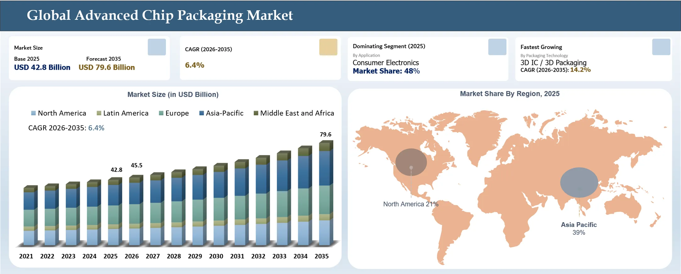
The global advanced chip packaging market was valued at approximately USD 42.8 billion in 2025 and is projected to reach around USD 79.6 million by 2035, expanding at a CAGR of approximately 6.4% during 2025–2035. The advanced chip packaging market is experiencing significant growth driven by the rapid expansion of artificial intelligence (AI) and high-performance computing (HPC), increasing adoption of high-bandwidth memory (HBM), growing use of chiplet-based architectures, the limitations of conventional semiconductor scaling, and the need for higher bandwidth and greater computing performance.
Growing demand for HBM to support AI accelerators is driving semiconductor manufacturers to expand advanced packaging capacity. This trend is encouraging large investments in dedicated HBM packaging facilities. For instance, in August 2026, SK hynix announced a $4 billion advanced HBM packaging facility in Indiana. The facility is expected to begin mass production in Q3 2029, with annual capacity expected to reach hundreds of thousands of wafers. The project is supported by $458 million in U.S. government grants and $500 million in loans.
Chiplets and Heterogeneous Packaging Are Changing System Design and Analysis
Advances in chip packaging are changing the semiconductor industry's focus from large, single-chips to systems made up of various small chips, referred to as chiplets, that are packaged together. This technology, termed heterogeneous integration, involves building various chiplets through different techniques and integrating them in order to gain advantages in flexibility, affordability, efficiency, and manufacturing yield.
Advanced packaging strategies include 2.5D packaging, which involves packing chiplets side by side on an interposer, and 3D packaging, which entails stacking of chips. For instance, TSMC’s CoWoS technology can integrate multiple chiplets and high-bandwidth memory (HBM) in a single package for AI and high-performance computing applications, demonstrating how packaging has become an important part of overall system design.
The chiplets-based designs can also allow companies to reuse their existing chip designs and choose various process nodes for performing various functions. As a consequence, advanced packaging becomes a important method of increasing the performance of systems, reducing development expenses, and achieving higher chip integration.
Advanced Chip Packaging Market Key Takeaways
- Asia Pacific held the leading regional market share, accounting for approximately 39% of the global advanced chip packaging market in 2025, supported by the region’s strong semiconductor manufacturing ecosystem, high concentration of foundries and OSAT providers, growing HBM production, and increasing investments in advanced packaging capacity. Countries such as Taiwan, South Korea, China, and Japan have established semiconductor and packaging capabilities, while rising demand for AI, high-performance computing, and data-center processors is further strengthening regional demand for advanced packaging technologies.
- Consumer electronics continues to represent the largest application segment in the global advanced chip packaging market, accounting for approximately 48% of market revenue in 2025, supported by high-volume demand for smartphones, laptops, tablets, wearables, and other connected devices. The increasing integration of processors, memory, RF components, and power-management components into compact devices is sustaining demand for advanced packaging technologies.
- Advancements in 2.5D and 3D integration, chiplet architectures, heterogeneous integration, and high-density interconnect technologies are becoming key strategic focus areas in the global advanced chip packaging market. Companies are increasingly investing in chiplet integration, silicon interposers, hybrid bonding, HBM integration, advanced substrates, thermal management, and high-density packaging processes to support increasingly complex AI and HPC semiconductor designs.
Advanced Chip Packaging Market Industry Trends and Strategic Insight
- Semiconductor companies, foundries, and OSAT providers are increasing investments in next-generation advanced packaging technologies to support increasingly complex AI, HPC, data-center, automotive, and consumer semiconductor devices. Companies are expanding capabilities in 2.5D and 3D packaging, chiplet integration, hybrid bonding, fan-out packaging, and heterogeneous integration.
- Demand for application-specific and customized packaging architectures is becoming a major market trend as different semiconductor applications require varying levels of computing performance, memory bandwidth, power efficiency, thermal management, and package size. This is increasing the adoption of specialized packaging solutions integrating processors, chiplets, HBM, and other components.
- The expansion of advanced packaging manufacturing capacity is accelerating the development of next-generation semiconductor supply chains. Rising demand for AI accelerators, high-performance processors, and HBM is encouraging foundries, IDMs, and OSAT companies to invest in new facilities, panel-level packaging, automated production lines, and domestic packaging ecosystems.
- Increasing focus on thermal management and power delivery is reshaping advanced chip packaging design. Higher power densities in AI accelerators and HBM-integrated devices are driving the development of improved thermal interface materials, heat spreaders, cooling solutions, and advanced power-delivery architectures.
Advanced Chip Packaging Market Scope
| Metrics | Details | |
| 2025 Market Size | USD 42.8 Billion | |
| 2035 Projected Market Size | USD 79.6 Billion | |
| CAGR (2026-2035) | 6.4% | |
| Largest Market | Asia-Pacific | |
| Fastest Growing Market | North America | |
| By Packaging Technology | Flip-Chip Packaging, Wafer-Level Packaging, 2.5D Packaging, 3D IC / 3D Packaging, System-in-Package (SiP), Embedded Die Packaging, Chiplet-Based Packaging, Other Advanced Packaging Technologies | |
| By Device Type | Logic Devices, Memory Devices, Analog & Mixed-Signal ICs, Power Devices, Sensors & MEMS, RF & Wireless Devices, Others | |
| By Material | Organic Materials, Silicon Materials, Ceramic Materials, Epoxy & Encapsulation Materials, Other Materials | |
| By Application | Artificial Intelligence (AI) & High-Performance Computing (HPC), Data Centers & Cloud Computing, Consumer Electronics, Automotive Electronics, Telecommunications, Industrial & IoT, Healthcare & Medical Devices, Aerospace & Defense | |
| By Region | North America | U.S., Canada, Mexico |
| Europe | Germany, United Kingdom, France, Italy, Spain, Netherlands, Switzerland, Sweden, Norway, Denmark, Belgium, Poland, Austria, Ireland, Portugal, Greece, Finland, and Rest of Europe. | |
| Asia-Pacific | China, Japan, India, South Korea, Australia, New Zealand, Singapore, Malaysia, Thailand, Indonesia, Vietnam, Philippines, Taiwan, and Rest of Asia Pacific. | |
| Latin America | Brazil, Argentina, Chile, Colombia, Peru, and Rest of Latin America. | |
| Middle East and Africa | Saudi Arabia, United Arab Emirates, Qatar, Kuwait, Oman, Bahrain, South Africa, Egypt, Nigeria, Morocco, and Rest of Middle East & Africa. | |
| Report Insights Covered | Competitive Landscape Analysis, Company Profile Analysis, Market Size, Share, Growth | |
Advanced Chip Packaging Market Disruption Analysis
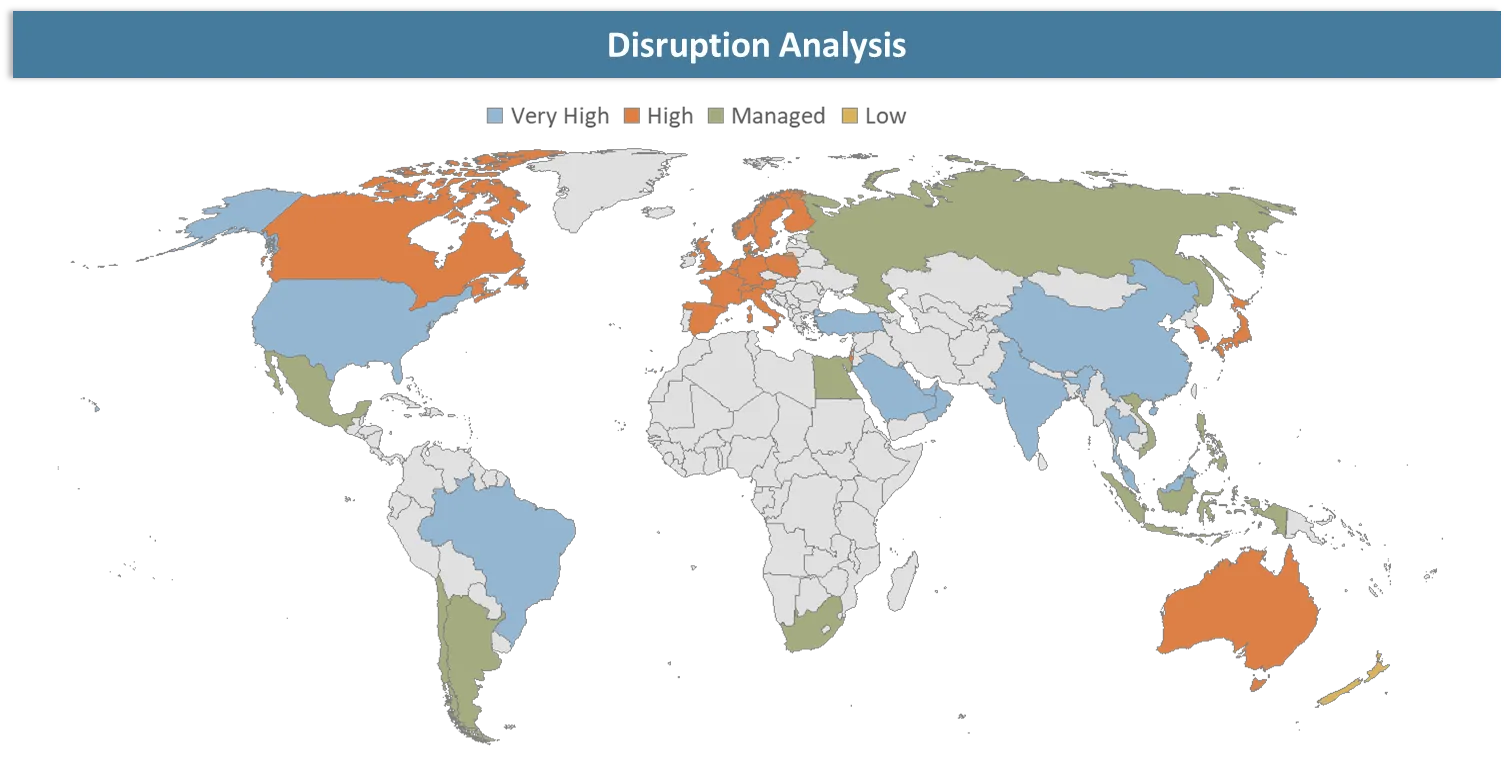
Shift From Wafer-Based Packaging Toward Panel-Level Packaging
The global advanced chip packaging market is witnessing a shift toward panel-level packaging (PLP), which has the potential to improve the manufacturing efficiency of semiconductor packaging by increasing throughput, improving material utilization, and enabling more packages to be processed simultaneously. This shift is encouraging packaging companies to develop large-format panel processing, advanced molding, redistribution layers, and automated assembly technologies to improve packaging throughput and manufacturing efficiency.
For instance, in May 2026, ASE Technology Holding announced an automated 310 × 310 mm panel-level packaging production line, with production expected to begin in the first half of 2027. ASE stated that the larger panel format can provide greater usable area, higher throughput, and improved material efficiency compared with traditional wafer-based processing. The investment demonstrates the industry's movement toward larger-format packaging processes to support increasing package sizes and improve manufacturing efficiency.
Advanced Chip Packaging Market BCG Matrix: Company Evaluation
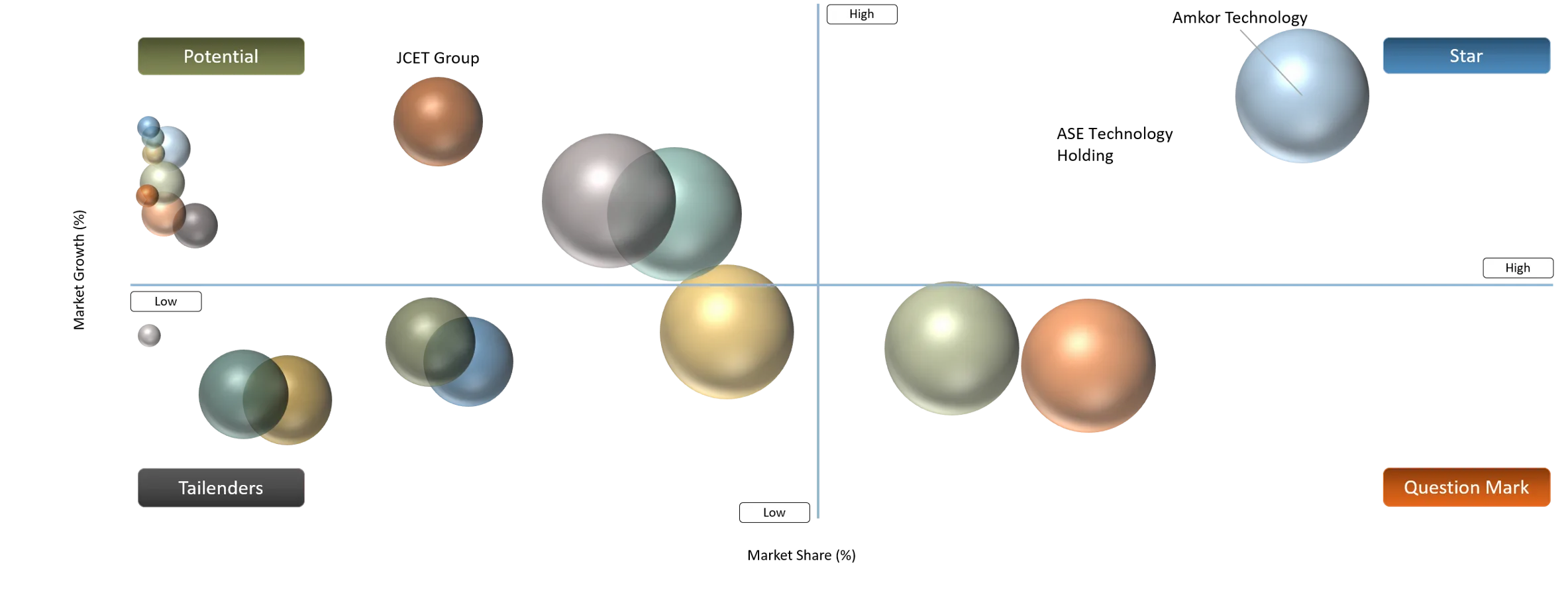
ASE Technology Holding Co., Ltd., Taiwan Semiconductor Manufacturing Company Limited (TSMC), Intel Corporation, Samsung Electronics Co., Ltd., and Amkor Technology, Inc. are classified as Star competitors due to their strong advanced packaging capabilities, significant investments in manufacturing capacity, proprietary packaging technologies, and broad involvement in AI, high-performance computing, data centers, HBM, and heterogeneous semiconductor integration.
These companies maintain strong market positions through technologies such as 2.5D and 3D packaging, chiplet integration, fan-out packaging, silicon interposers, and advanced memory packaging. JCET Group, Tongfu Microelectronics Co., Ltd., Powertech Technology Inc., Huatian Technology, and SK hynix Inc. are categorized as high-growth players, supported by expanding advanced packaging capacity, increasing demand for AI and HBM-related semiconductor packaging, and growing investments in high-density integration, memory packaging, and advanced assembly and testing technologies. Their growth is further supported by the expansion of domestic semiconductor supply chains, particularly in Asia Pacific.
Texas Instruments Inc. and Qualcomm Inc. represent established/specialized competitors, driven by their strong semiconductor design and manufacturing capabilities and increasing adoption of advanced packaging solutions for application-specific devices. Their positions are supported by demand across automotive, industrial, telecommunications, consumer electronics, and high-performance computing applications, although advanced packaging services are not their primary standalone business compared with leading foundries and OSAT providers.
Advanced Chip Packaging Market Dynamics
Driver Impact Analysis
| Driver | Market Growth Impact (%) | Demand Concentration | Impacted Use Case | Strategic Impact |
Rapid Growth in Artificial Intelligence and High-Performance Computing | 30% | Strong demand concentration in North America and Asia Pacific, particularly in the United States, Taiwan, South Korea, China, and Japan, supported by expanding AI infrastructure and semiconductor investments. | AI accelerators, GPUs, HPC processors, HBM-integrated devices, and generative AI infrastructure. | Increases demand for advanced packaging technologies capable of integrating multiple compute dies, chiplets, HBM, and high-density interconnects within high-performance semiconductor packages. |
Increasing Adoption of Chiplet Architectures and Heterogeneous Integration | 25% | Strong technology adoption among leading semiconductor companies in the United States, Taiwan, South Korea, and China, with growing relevance across global HPC, data-center, and specialized semiconductor markets. | Multi-chip processors, AI accelerators, CPUs, GPUs, networking chips, and application-specific integrated circuits. | Drives the transition from monolithic semiconductor designs toward multi-die integration, increasing demand for 2.5D and 3D packaging, silicon interposers, hybrid bonding, and advanced interconnect technologies. |
Rising Demand for High-Bandwidth Memory and Advanced Memory Integration | 20% | High demand concentration in South Korea, Taiwan, the United States, and other major AI semiconductor manufacturing hubs, supported by growing production of AI accelerators and data-center processors. | HBM-integrated GPUs, AI accelerators, HPC systems, and data-center processors. | Expands demand for advanced memory packaging and high-density stacking technologies capable of delivering greater memory bandwidth, capacity, and power efficiency. |
Expansion of Data Centers and Cloud Computing Infrastructure | 15% | Strongest demand in North America and Asia Pacific, supported by hyperscale cloud providers, AI data-center investments, and digital infrastructure expansion. | Servers, data-center processors, networking chips, AI accelerators, and cloud computing hardware. | Supports higher demand for high-performance and power-efficient semiconductor packages capable of managing increased computing workloads, thermal requirements, and memory bandwidth. |
Government Support for Domestic Semiconductor Manufacturing and Supply-Chain Localization | 10% | Strong policy and investment activity across the United States, Europe, China, Japan, South Korea, and other strategic semiconductor manufacturing regions. | Domestic semiconductor manufacturing, advanced packaging facilities, assembly and testing operations, and semiconductor R&D. | Encourages investment in regional advanced packaging capacity, strengthens domestic semiconductor supply chains, and supports the development of new packaging facilities and technology ecosystems. |
Accelerating AI Infrastructure Increasing Demand for Advanced Packaging
The rapid expansion of AI, generative AI, accelerated computing, and AI data centers is driving demand for increasingly complex semiconductor devices, which in turn is increasing the need for advanced chip packaging technologies capable of integrating high-performance processors, HBM, multiple dies, and high-density interconnections within a single package.
The strong growth of AI infrastructure is reflected in the financial performance of major semiconductor and AI technology companies, indicating continued expansion in demand for AI accelerators, data-center processors, and networking semiconductors. NVIDIA's fiscal 2026 revenue reached $215.9 billion, increasing 65% year over year, while its Data Center business increased 68% year over year, reflecting strong demand for accelerated computing and AI infrastructure.
Similarly, Broadcom reported $16.7 billion in AI semiconductor revenue in Q3 FY2026, more than tripling year over year, driven by demand for custom AI accelerators and networking products, the company subsequently raised its expected AI chip revenue to approximately $115 billion for FY2027.
Restraint Impact Analysis
| Restraint | Drag on Market Growth (%) | Primary Impact Area | Impacted Use Case | Strategic Impact |
High Capital Investment and Advanced Packaging Manufacturing Costs | 30% | Advanced packaging equipment, cleanroom facilities, lithography systems, bonding equipment, substrates, interposers, testing infrastructure, and process development. | 2.5D and 3D packaging, chiplet integration, HBM packaging, fan-out packaging, and heterogeneous integration. | High upfront investment requirements can limit market entry and capacity expansion, particularly for smaller OSAT providers and semiconductor manufacturers. |
Technical Complexity and Manufacturing Yield Challenges | 25% | Multi-die integration, high-density interconnects, wafer bonding, die stacking, package warpage, thermal management, and defect control. | AI accelerators, HPC processors, HBM-integrated devices, and complex multi-chip semiconductor packages. | Low manufacturing yields and technical integration challenges can increase production costs, reduce scalability, and delay the commercialization of advanced packaging technologies. |
Limited Advanced Packaging Capacity and Supply-Chain Constraints | 20% | Availability of advanced packaging facilities, substrates, interposers, bonding equipment, packaging materials, and specialized manufacturing equipment. | AI chips, GPUs, HBM-integrated processors, data-center semiconductors, and high-performance computing devices. | Capacity shortages and supply-chain bottlenecks can extend lead times, increase packaging costs, and limit the production of high-demand advanced semiconductor devices. |
Thermal Management and Power Density Challenges | 15% | Heat dissipation, power delivery, package reliability, thermal interface materials, cooling systems, and high-density semiconductor architectures. | AI accelerators, GPUs, HPC processors, and high-power data-center chips. | Increasing power density creates significant thermal and reliability challenges, requiring additional investment in cooling, materials, and package design technologies. |
Complex Ecosystem Integration and Design Requirements | 10% | Coordination between foundries, OSAT providers, chip designers, substrate suppliers, memory manufacturers, and equipment companies. | Chiplet-based systems, heterogeneous integration, system-in-package, and multi-vendor semiconductor architectures. | Complex co-design and interoperability requirements can increase development timelines and engineering costs while making supply-chain coordination more challenging. |
High Capital Investment and Advanced Packaging Manufacturing Costs
Advanced chip packaging requires substantial investment in specialized manufacturing infrastructure, including cleanroom facilities, advanced bonding and lithography equipment, inspection and testing systems, high-precision assembly tools, silicon interposers, advanced substrates, and thermal-management materials. Technologies such as 2.5D and 3D packaging, hybrid bonding, chiplet integration, and HBM packaging involve significantly higher process complexity and equipment requirements than conventional semiconductor packaging.
These high capital requirements can create barriers for smaller OSAT providers and new market entrants while increasing the financial risks associated with expanding advanced packaging capacity. Major companies including TSMC, ASE Technology Holding, Amkor Technology, Samsung Electronics, Intel Corporation, JCET Group, and SK hynix are investing in advanced packaging technologies and manufacturing capacity to address growing demand from AI, HPC, and data-center applications.
Advanced Chip Packaging Market Segment Analysis
The global advanced chip packaging market is segmented based on packaging technology, device type, material, application, and region.
Rising Semiconductor Integration and Miniaturization Requirements Support Market Dominance of Consumer Electronics
Consumer Electronics is expected to account for the dominant share of the global advanced chip packaging market in 2025, driven by the high-volume production of smartphones, tablets, laptops, wearables, and other connected electronic devices. Advanced packaging technologies are widely used in consumer devices to enable smaller form factors, higher processing performance, improved power efficiency, and greater component integration.
Consumer electronics manufacturers are increasingly adopting advanced packaging technologies to achieve higher performance and functionality within compact device designs. For instance, in August 2024, Samsung Electronics began mass production of its 12nm-class LPDDR5X DRAM packages for mobile applications.
The packages stack four layers of DRAM dies within a 0.65-mm-high package, enabling higher memory density while improving thermal characteristics and freeing space inside mobile devices. This demonstrates how advanced packaging is being used in consumer electronics to increase functionality and memory capacity within increasingly space-constrained devices.
Advanced Chip Packaging Market Geographical Penetration
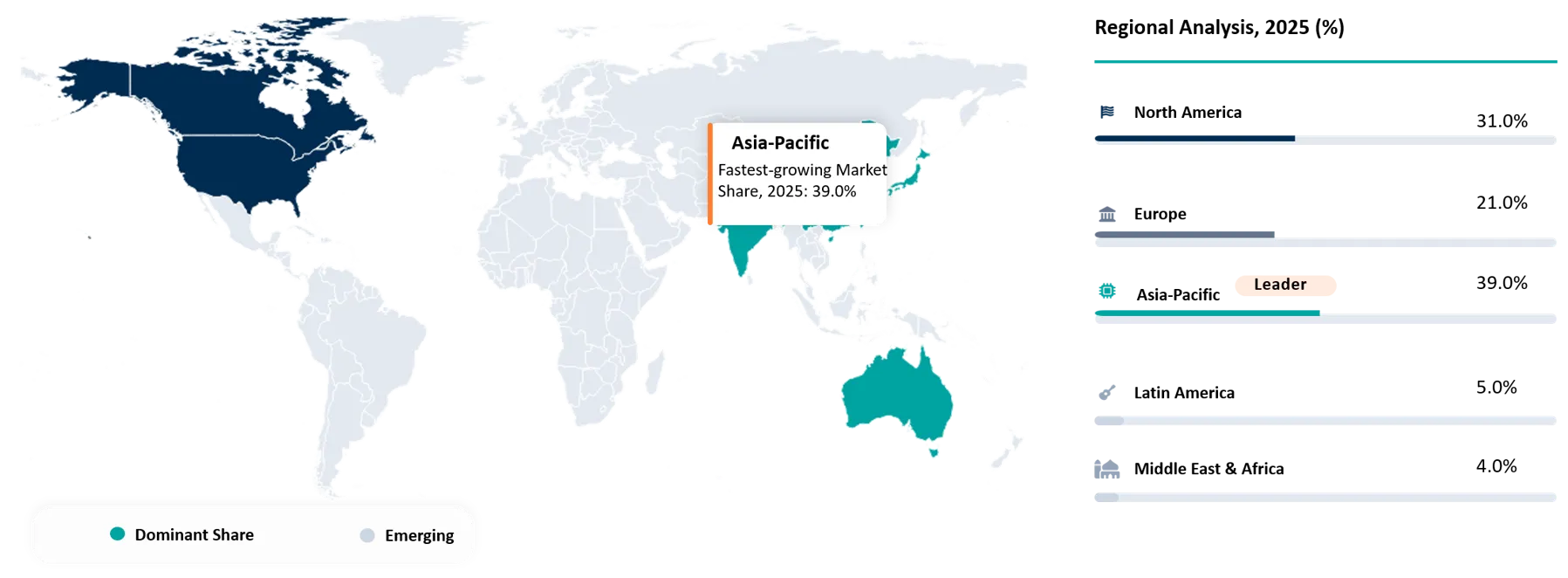
Government Support and Advanced Packaging Investments Drive Growth in North America
North America is expected to represent a significant market for advanced chip packaging, driven primarily by strong demand for artificial intelligence (AI), high-performance computing (HPC), cloud data centers, and next-generation semiconductor technologies. The region benefits from the presence of major semiconductor and technology companies, increasing government support for domestic semiconductor supply chains, and substantial investments in advanced packaging and testing infrastructure.
For instance, in November 2025, the Government of Canada announced up to US$150 million in federal funding toward an approximately US$473 million project to expand semiconductor packaging and commercialization capabilities at IBM Canada's Bromont facility and the MiQro Innovation Collaborative Centre (C2MI) in Quebec. The project is intended to bring new advanced packaging and R&D capabilities for next-generation semiconductors to Canada, supporting applications including AI and high-performance computing.
Government Support and Domestic Advanced Packaging Investments Drive US Market Growth
The US is emerging as a key hub for advanced chip packaging, driven by strong demand for AI, high-performance computing (HPC), data centers, and advanced semiconductor technologies, along with substantial government and private-sector investments aimed at strengthening domestic packaging capabilities. The country's growth is supported by the CHIPS and Science Act and the National Advanced Packaging Manufacturing Program (NAPMP), which specifically focuses on expanding domestic advanced packaging research, development, and manufacturing.
The United States is also witnessing significant investments in commercial advanced packaging capacity. For instance, Amkor Technology is investing approximately US$7 billion across two phases to develop an advanced semiconductor packaging and test campus in Arizona, which is expected to become the first high-volume advanced packaging OSAT facility in the United States. The U.S. Department of Commerce has also awarded Amkor up to US$407 million in CHIPS Act funding for the project.
Strong Semiconductor Manufacturing and Packaging Infrastructure Positions Asia Pacific as a Market Leader
Asia Pacific is expected to hold a leading position in the global advanced chip packaging market, supported by its strong semiconductor manufacturing and packaging ecosystem, particularly in South Korea, China, Taiwan, and Japan. The region's growth is driven by increasing AI and high-performance computing demand, HBM production, expansion of OSAT capacity, chiplet adoption, and government investments in semiconductor manufacturing and advanced packaging infrastructure. The presence of major companies such as Samsung Electronics, SK hynix, ASE, TSMC, JCET, and Tongfu further strengthens the region's advanced packaging capabilities.
Strong Semiconductor Manufacturing Capabilities Position South Korea as a Key Advanced Packaging Hub
South Korea is anticipated to hold a considerable proportion of the Asia Pacific advanced chip packaging market, owing to the country's semiconductor manufacturing industry and leading position in advanced memory technologies. South Korea's growth is primarily due to the fast-growing AI and high-performance computing (HPC), rising demand for high-bandwidth memory (HBM), and further investments in advanced semiconductor packaging plants.
South Korea houses leading semiconductor firms such as Samsung Electronics and SK hynix, which are working on 3D memory stacking, HBM packaging, hybrid bonding, and advanced thermal management technology. For instance, in January 2026, SK hynix announced that it would be investing around KRW 19 trillion (US$12.9 billion) in the construction of an advanced semiconductor packaging plant in South Korea.
The construction work began in April 2026 and be completed by December 2027. The aim of the investment is to increase the capacity of the company in advanced packaging technology and meet the growing demand for AI memory and more specifically HBM memory.
Government Support and Semiconductor Ecosystem Drive Advanced Packaging Growth in Japan
Japan is anticipated to have a major share in the Asia Pacific advanced chip packaging market, considering its already developed semiconductor industry, dominance in semiconductor materials and equipment, and growing investments in advanced packaging and domestic semiconductor production. The factors driving the growth of Japan’s market are growing demand for artificial intelligence (AI) and HPC, use of heterogenous integration and chiplets, and efforts to boost the domestic semiconductor value chain in Japan.
The Japanese government has been making substantial investments to build a robust semiconductor industry in Japan, including advanced packaging. For instance, in February 2026, Rapidus received a US$645 million investment from Japan's Information-technology Promotion Agency (IPA), followed by an additional US$967 million investment in June 2026.
The government-backed funding supports Rapidus's development of next-generation semiconductor technologies, while its government-supported R&D programs include the “Development of Chiplet, Package Design and Manufacturing Technology for 2nm-Generation Semiconductors,” directly supporting Japan's advanced semiconductor packaging ecosystem.
Advanced Chip Packaging Market Competitive Landscape
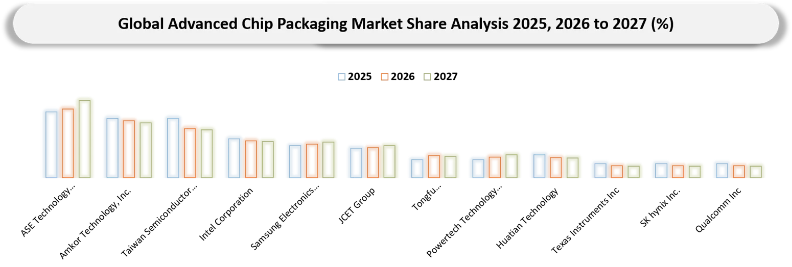
- The global advanced chip packaging market is characterized by the presence of semiconductor foundries, outsourced semiconductor assembly and test (OSAT) companies, integrated device manufacturers (IDMs), and semiconductor companies developing advanced packaging technologies for high-performance computing, artificial intelligence (AI), data centers, memory, automotive, and consumer electronics applications.
- ASE Technology Holding Co., Ltd., Amkor Technology, Inc., Taiwan Semiconductor Manufacturing Company Limited (TSMC), Intel Corporation, Samsung Electronics Co., Ltd., JCET Group, Tongfu Microelectronics Co., Ltd., Powertech Technology Inc., Huatian Technology, Texas Instruments Inc., SK hynix Inc., and Qualcomm Inc. are among the notable players due to their advanced packaging capabilities and involvement in technologies such as 2.5D and 3D integration, chiplet packaging, fan-out packaging, wafer-level packaging, high-density interconnects, and heterogeneous integration.
- TSMC and Intel maintain strong positions through proprietary advanced packaging platforms, including CoWoS, SoIC, EMIB, and Foveros, while ASE Technology Holding and Amkor Technology are major OSAT companies expanding their advanced packaging and testing capabilities. Samsung Electronics and SK hynix contribute through advanced memory and HBM packaging technologies, whereas JCET Group, Tongfu Microelectronics, Powertech Technology, and Huatian Technology participate through semiconductor assembly, testing, wafer-level packaging, and advanced packaging services.
- Meanwhile, Texas Instruments and Qualcomm are involved in the development and adoption of advanced semiconductor packaging solutions for high-performance and application-specific semiconductor devices.
- ASE Technology Holding Co., Ltd. (Taiwan), Amkor Technology, Inc. (United States), Taiwan Semiconductor Manufacturing Company Limited (TSMC) (Taiwan), Intel Corporation (United States), Samsung Electronics Co., Ltd. (South Korea), JCET Group (China), Tongfu Microelectronics Co., Ltd. (China), Powertech Technology Inc. (Taiwan), Huatian Technology (China), Texas Instruments Inc. (United States), SK hynix Inc. (South Korea), and Qualcomm Inc. (United States) are among the notable players operating in the global advanced chip packaging market.
Key Developments
- June 2026, JCET announced plans to invest approximately US$1.15 billion to build a new advanced semiconductor packaging and testing facility in Shanghai. The project will be developed in two phases, with the first phase, covering factory construction and equipment investment, scheduled for completion in the second half of 2028. The investment is aimed at expanding JCET's high-end advanced packaging capacity amid growing demand for domestic semiconductors and AI-related chips in China.
- July 2026, Samsung Electronics and Broadcom signed a memorandum of understanding to expand their strategic collaboration across memory, foundry, and advanced packaging technologies for next-generation AI infrastructure. The collaboration, estimated at more than US$200 billion over the next five years through 2030, includes the supply of HBM for Broadcom's AI accelerators and the development of advanced packaging technologies, including 2.3D and 2.5D integration, based on Samsung's 2 nm process technology to support higher-performance and more power-efficient AI and networking semiconductors.
- January 2026: SK hynix announced plans to invest approximately KRW 19 trillion (US$12.9 billion) to build an advanced semiconductor packaging plant in South Korea. Construction of the facility is scheduled to begin in April 2026, with completion targeted by the end of 2027. The investment is intended to expand the company's advanced packaging capabilities and address growing demand for AI-focused memory, particularly High-Bandwidth Memory (HBM).
- August 2026: SK hynix announced a $4 billion advanced HBM packaging facility in Indiana. The facility is expected to begin mass production in Q3 2029, with annual capacity expected to reach hundreds of thousands of wafers. The project is supported by $458 million in U.S. government grants and $500 million in loans.
Key Procurement Priorities and Buyer Evaluation Criteria
- Buyers prioritize advanced chip packaging solutions with proven performance in high-density semiconductor integration, electrical reliability, thermal management, and power efficiency to meet the requirements of applications such as AI, high-performance computing, data centers, consumer electronics, automotive, and telecommunications.
- Buyers prioritize packaging technologies capable of supporting high-density interconnects, multiple dies, chiplets, HBM, heterogeneous integration, and advanced memory configurations while maintaining package reliability and performance.
- Evaluation is based on criteria such as interconnect density, package size, I/O density, signal integrity, power delivery, thermal performance, memory bandwidth, package warpage, reliability, yield, and compatibility with different semiconductor process technologies.
- Buyers consider factors including packaging technology capabilities, manufacturing capacity, production yield, scalability, turnaround time, quality consistency, testing capabilities, defect rates, and the supplier's ability to support high-volume semiconductor production.
- Preference is given to suppliers with expertise in 2.5D and 3D packaging, fan-out packaging, chiplet integration, wafer-level packaging, hybrid bonding, silicon interposers, advanced substrates, HBM integration, and heterogeneous semiconductor integration.
- Semiconductor companies and system manufacturers particularly prioritize suppliers with proven commercial-scale manufacturing capabilities, advanced packaging capacity, strong quality-control systems, technical support, design collaboration capabilities, and reliable semiconductor supply chains.
- Buyers also evaluate supplier capabilities related to package co-design, simulation, testing, failure analysis, thermal engineering, and compatibility with foundry, memory, substrate, and assembly processes, as advanced packaging increasingly requires close collaboration across the semiconductor ecosystem.
- Cost considerations include packaging and assembly costs, substrate and material costs, equipment requirements, production yield, testing expenses, development costs, and total cost per packaged semiconductor. Suppliers that can provide high manufacturing yields, scalable production capacity, reliable performance, and competitive packaging costs are generally preferred.
Why Choose DataM?
- Technological Innovations: Explores advancements in advanced chip packaging technologies, including 2.5D and 3D packaging, chiplet integration, heterogeneous integration, fan-out packaging, wafer-level packaging, hybrid bonding, silicon interposers, advanced substrates, high-density interconnects, HBM integration, and thermal-management solutions that improve semiconductor performance, bandwidth, power efficiency, and component integration.
- Product Performance & Market Positioning: Evaluates how semiconductor companies, foundries, IDMs, and OSAT providers differentiate their advanced packaging solutions based on interconnect density, package size, I/O density, memory bandwidth, thermal performance, power efficiency, manufacturing yield, reliability, scalability, and suitability for applications such as AI, HPC, data centers, consumer electronics, automotive, telecommunications, and industrial systems.
- Real-World Evidence: Highlights commercial deployments and adoption of advanced packaging technologies across AI accelerators, GPUs, CPUs, HBM-integrated processors, automotive semiconductors, and consumer electronic devices, demonstrating benefits such as higher computing performance, increased memory bandwidth, reduced package size, improved power efficiency, and greater integration of multiple semiconductor dies.
- Market Updates & Industry Changes: Tracks key developments including new advanced packaging technologies, manufacturing facility expansions, capacity investments, semiconductor product introductions, panel-level packaging developments, HBM packaging advancements, government funding, strategic partnerships, technology collaborations, and investments across major semiconductor markets such as Asia Pacific, North America, and Europe.
- Competitive Strategies: Analyzes how leading companies expand through investments in advanced packaging capacity, development of proprietary packaging platforms, partnerships between foundries and semiconductor companies, expansion of HBM and chiplet integration capabilities, technology collaborations, geographic expansion, and development of application-specific packaging solutions.
- Pricing & Market Access: Explains cost variations based on packaging technology, package complexity, number of integrated dies, substrate and interposer requirements, HBM integration, testing requirements, manufacturing volumes, production yield, thermal-management requirements, and customization. It also evaluates procurement models and supplier relationships involving foundries, OSAT providers, IDMs, fabless semiconductor companies, and technology partners.
- Market Entry & Expansion: Identifies growth opportunities driven by increasing demand for AI and HPC, expansion of data centers, rising adoption of chiplet architectures, HBM integration, automotive electrification, and semiconductor supply-chain localization, while outlining strategies such as advanced packaging capacity expansion, technology partnerships, government-supported manufacturing investments, regional production facilities, ecosystem collaboration, and application-specific packaging development.
Target Audience
- Semiconductor Manufacturers, Integrated Device Manufacturers (IDMs), Foundries, and Advanced Chip Packaging Companies
- Outsourced Semiconductor Assembly and Test (OSAT) Providers and Semiconductor Testing Companies
- Fabless Semiconductor Companies, Chip Designers, and AI Accelerator Developers
- Data Center, Cloud Computing, Artificial Intelligence (AI), and High-Performance Computing (HPC) Companies
- Semiconductor Equipment, Materials, Substrate, Interposer, and Packaging Technology Suppliers
- Consumer Electronics, Automotive Electronics, Telecommunications, Industrial, Aerospace, and Defense Semiconductor Manufacturers
- Research Institutions, Universities, Government Organizations, and Semiconductor Research Centers focused on Advanced Packaging and Heterogeneous Integration
- Investors, Venture Capital Firms, Private Equity Firms, Government Funding Agencies, and Strategic Partners evaluating Advanced Semiconductor and Chip Packaging Technologies