3D IC Market Size and Overview
The global 3D IC market was valued at approximately US$ 19.46 billion in 2025 and is projected to reach about US$ 67.1 billion by 2035, expanding at an estimated CAGR of approximately 13.2% during 2026-2035. Demand is accelerating as advanced processors, high-bandwidth memory, chiplets, mobile devices and automotive electronics require more compute and memory bandwidth within tighter power and footprint limits.
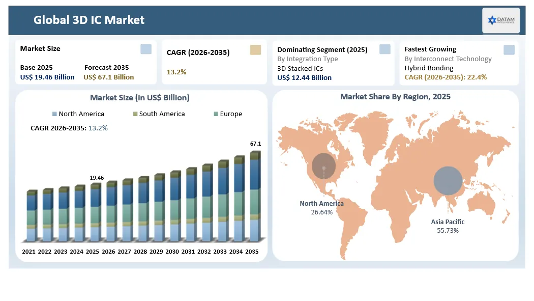
The market entered 2026 with strong investment momentum. TSMC reported Q2 2026 net revenue of US$40.20 billion, while Amkor reported record Q2 2026 net sales of US$1.90 billion, up 26% year over year. Intel also highlighted rising demand for wafer and advanced packaging offerings in Q1 2026, reinforcing the strategic importance of heterogeneous integration and advanced assembly.
| Metric | Details |
| 2025 Market Size | US$ 19.46 Billion |
| 2035 Projected Market Size | US$ 67.1 Billion |
| CAGR (2026-2035) | 13.2% |
| Largest Market | Asia-Pacific |
| Fastest Growing Market | North America / Asia-Pacific |
| Dominating Integration Type | 3D Stacked ICs |
| Fastest Growing Technology | Hybrid Bonding |
| Primary Growth Engine | AI/HPC, HBM and chiplet-based heterogeneous integration |
3D IC Market Key Takeaways
- TSV-based 3D stacking remains a foundational technology, while hybrid bonding is emerging as the next major interconnect transition for finer pitch, lower power and higher bandwidth.
- HBM is one of the largest near-term demand engines because advanced processors require vertically stacked DRAM tightly integrated with advanced logic packages.
- Foundry-integrated packaging and OSAT capacity are becoming strategic assets as customers compete for CoWoS-class, wafer-level and advanced 3D assembly slots.
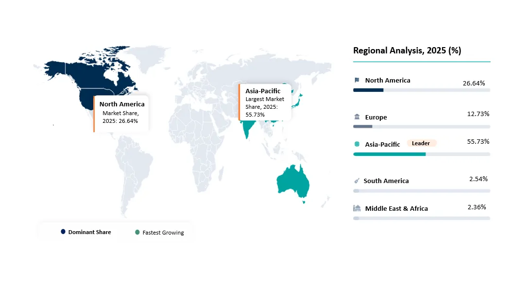
- Asia-Pacific dominates manufacturing capacity through Taiwan, South Korea, China, Japan and Southeast Asia, while North America leads many AI/HPC design programs and semiconductor equipment technologies.
- Chiplets, hybrid bonding, glass interposers, backside power and 3D logic-on-logic integration are reshaping semiconductor scaling beyond conventional monolithic die growth.
- Yield learning, thermal density, known-good-die testing and package warpage remain critical barriers to broader 3D integration.
- Buyer decisions increasingly emphasize bandwidth density, energy per bit, package yield, thermal resistance, assembly capacity and long-term technology-roadmap compatibility.
- The market ecosystem is tightly coupled across EDA, wafer fabrication, bonding equipment, TSV processes, interposers, substrates, OSATs, memory suppliers and end-device designers.
3D IC Industry Trends and Strategic Insights
- The semiconductor industry is shifting from transistor scaling alone toward system-level scaling using chiplets, 2.5D/3D integration and vertically stacked memory. Performance gains increasingly come from shortening die-to-die interconnects and integrating specialized dies within one package.
- TSMC, Samsung and Intel are expanding foundry-integrated advanced packaging, while ASE and Amkor scale outsourced packaging capacity. Memory suppliers are advancing HBM3E and HBM4 stacks that require increasingly complex 3D assembly and thermal design.
- Hybrid bonding is moving from image sensors and selected memory applications toward logic and advanced compute, enabling finer pitches than conventional micro-bumps and improving bandwidth density.
- 3D integration is broadening from high-end data-center systems into smartphones, automotive processors, sensors, RF modules, photonics and industrial edge devices as package density requirements increase.
- Supply-chain advantage increasingly depends on access to advanced lithography, bonding and metrology tools, high-quality wafers and interposers, substrates, underfill materials and experienced assembly capacity.
- Government semiconductor incentives in the U.S., Europe, Japan, South Korea, Taiwan and other regions are supporting local advanced packaging and heterogeneous-integration capability.
3D IC Market Scope
| Metrics | Details |
| By Integration Type | 3D Stacked ICs; Monolithic 3D ICs; 2.5D/3D Heterogeneous Integration; 3D Wafer-Level Integration; Other |
| By Interconnect Technology | Through-Silicon Via (TSV); Hybrid Bonding; Micro-bump / Cu Pillar; Through-Glass Via (TGV); Other |
| By Product / Component | 3D Memory; Logic / Processors; MEMS / Sensors / Imaging; RF / Analog / Photonics; Other |
| By Bonding / Stacking Method | Die-to-Wafer; Wafer-to-Wafer; Die-to-Die; Chiplet / Heterogeneous Package Integration |
| By Application | AI / HPC & Data Centers; Consumer Electronics & Smartphones; Automotive Electronics; Networking / Telecom & Edge; Medical & Imaging; Other |
| By End Use Industry | IT & Telecommunications; Consumer Electronics; Automotive; Healthcare; Aerospace & Defense; Industrial & IoT; Other |
| By Manufacturing Model | Foundry-Integrated Packaging; OSAT / Outsourced Packaging; IDM / Vertically Integrated; Fabless / Co-Design Partnerships; Equipment & Materials-Enabled Integration |
| By Material / Integration Platform | Silicon TSV / Interposer; Glass Interposer / TGV; Organic Substrate / Redistribution Layers; Hybrid Bonding & Advanced Dielectrics |
| By Region | North America; Europe; Asia-Pacific; South America; Middle East & Africa |
Why does this report matter in 2026?
The year 2026 marks a step-change in commercial 3D integration as AI systems drive unprecedented demand for HBM and advanced packages, while chiplet architectures move deeper into CPUs, accelerators, networking and automotive compute. Packaging is increasingly a performance technology rather than a back-end commodity.
The report matters because 3D IC competitiveness depends on an interdependent chain of foundries, memory suppliers, OSATs, bonding and metrology equipment, substrates and EDA. Capacity constraints or yield issues at any one layer can materially affect product launches and semiconductor economics.
3D IC Market White Space & Investment Opportunities
- Hybrid-bonding equipment and process capability for sub-10-micron and future sub-5-micron interconnect pitches.
- Advanced packaging capacity for HBM, advanced processors and chiplet-based compute systems.
- Glass interposers and TGV technologies for larger package sizes, improved dimensional stability and high-frequency performance.
- Thermal materials, microfluidic cooling and package-level heat-spreading solutions for dense 3D stacks.
- Known-good-die testing, 3D design verification and yield analytics that reduce the cost of multi-die integration.
- Automotive, photonics, medical imaging and sensor-fusion applications that can benefit from vertical heterogeneous integration.
3D IC Future Market Transformation
By 2035, 3D IC architectures are expected to evolve toward highly heterogeneous systems combining logic, memory, analog, RF, photonics and specialized accelerators in tightly integrated packages. Hybrid bonding and wafer-level stacking should reduce interconnect distance and enable far denser die-to-die connectivity.
Business models will converge. Foundries will bundle wafer fabrication and advanced packaging, OSATs will expand into higher-value co-design and wafer-level services, and equipment/material suppliers will capture more value from increasingly complex integration flows.
3D IC Market Buyer Decision-Making Criteria
Buyers prioritize interconnect pitch, bandwidth density, package yield, thermal performance, supported die size, HBM stack capability, substrate availability, test coverage, qualification history, capacity assurance and compatibility with chiplet/EDA ecosystems.
3D IC Market Economic & Investment Analysis
3D IC economics are shaped by wafer cost, die yield, TSV or bonding process steps, interposer/substrate cost, test complexity and package yield. The value proposition improves when 3D integration materially reduces power, increases bandwidth or allows expensive leading-edge logic to be combined with lower-cost mature-node chiplets.
Investment is increasing across advanced packaging fabs, hybrid-bonding tools, metrology, wafer thinning, temporary bonding, high-density substrates, HBM production and package-level thermal technologies. Bottleneck capacity can earn premium economics when AI/HPC demand is strong.
3D IC Investment Trends in the Market
- Foundries and OSATs are expanding advanced packaging and 3D integration capacity near major wafer-fab clusters.
- Memory suppliers are scaling HBM stack height, bandwidth and advanced bonding while aligning capacity with advanced processor roadmaps.
- Equipment vendors are investing in wafer bonding, thinning, deposition, inspection and metrology for tighter interconnect pitches.
- Substrate and interposer suppliers are pursuing larger formats, improved warpage control and glass-based alternatives.
- Partnerships increasingly link foundries, OSATs, equipment vendors and chip designers to qualify complete 3D integration flows.
Strategic Indicators For 3D IC Market
High Regulation Impact
Export controls, semiconductor incentives, technology-transfer rules and supply-chain security policies influence where advanced packaging tools, processes and leading-edge products can be manufactured or sold.
High Investment Activity
3D IC is attracting substantial capital across advanced packaging fabs, HBM lines, hybrid-bonding equipment, substrates, metrology and thermal solutions.
Supply Chain Disruption
Concentration in advanced packaging capacity, HBM, substrates and specialized equipment create allocation risk and can delay high-value semiconductor programs.
Pricing Volatility
Pricing varies with die count, stack height, interconnect density, interposer size, substrate availability, yield and qualification requirements. AI/HPC packages command a premium over conventional packaging.
Procurement Pressure
Buyers face pressure to reserve advanced packaging slots, secure HBM and substrates and qualify alternate assembly sites without compromising yield or reliability.
New Technology Adoption
Hybrid bonding, TGVs, chiplets, backside power delivery, HBM4, wafer-to-wafer stacking and thermal-aware 3D design are changing integration strategies.
Regional Expansion Opportunity
Asia-Pacific remains the manufacturing center, while North America, Europe and Japan are expanding domestic advanced packaging capacity and semiconductor ecosystem resilience.
Government Policy Support
CHIPS-style incentives and national semiconductor strategies increasingly include advanced packaging, substrates, R&D centers and heterogeneous-integration pilot lines.
Pricing Intelligence
Pricing is shifting from simple package cost toward system-level value, including bandwidth, power savings, yield, package area and time-to-market benefits.
Disruption Analysis of 3D IC Market
The market is being disrupted by hybrid bonding, chiplets, HBM, large silicon and glass interposers and foundry-integrated packaging. These shifts move value toward packaging platforms that can deliver wafer-scale precision, high yield and reliable thermal performance.
3D IC Market BCG Matrix: Company Evaluation
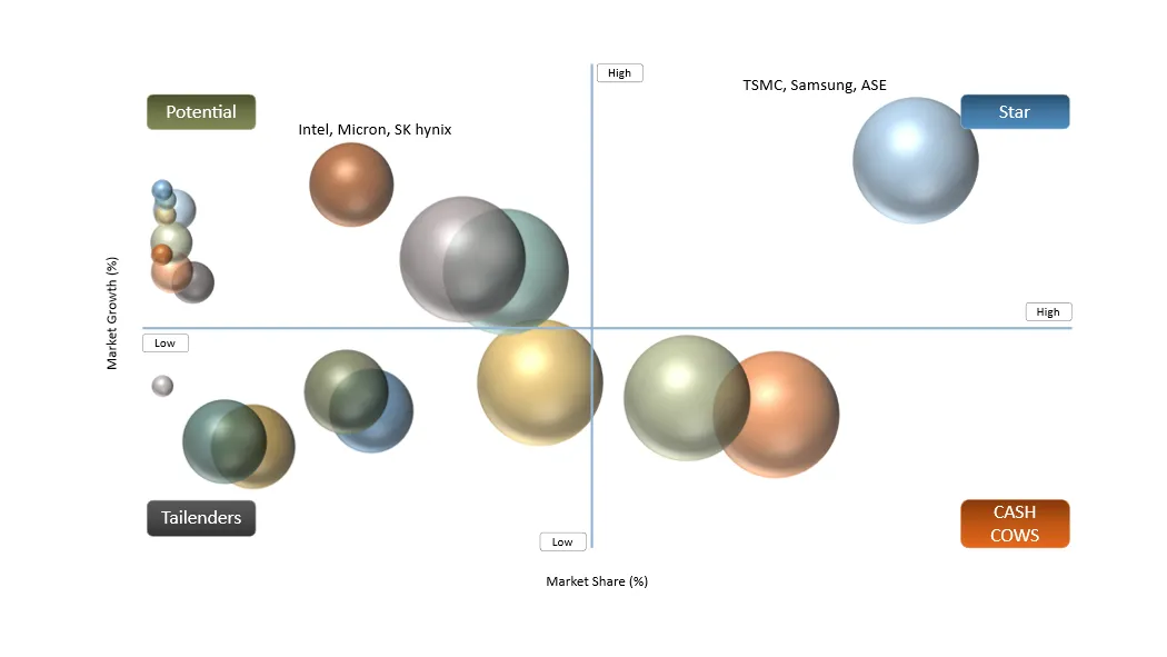
STAR
TSMC, Samsung, ASE and Amkor occupy the Star category because they combine large-scale semiconductor manufacturing or packaging capabilities with direct exposure to rapidly expanding AI/HPC and advanced integration demand.
POTENTIAL
Intel, Micron, SK hynix, Besi, Applied Materials and other equipment/material specialists remain high-potential participants as hybrid bonding, HBM and domestic advanced packaging investment expand.
3D IC Market Dynamics
Driver Impact Analysis
| Driver | Market Growth Impact | Demand Concentration | Impacted Use Case | Strategic Impact |
| AI/HPC and HBM expansion | Very High | Data centers and accelerator ecosystems | 3D memory and logic-memory integration | Accelerates demand for TSV, interposers and hybrid bonding |
| Chiplet architectures | Very High | CPU, GPU, networking and custom ASICs | Heterogeneous multi-die packages | Extends scaling while reducing dependence on monolithic die size |
| Device miniaturization | High | Mobile, automotive and sensors | MEMS, imaging and compact electronics | Increases value of vertical integration and wafer-level packaging |
| Government semiconductor investment | High | U.S., Europe and Asia | Domestic advanced packaging capacity | Supports new packaging fabs, pilot lines and supply-chain resilience |
Driver: AI/HPC, HBM and Chiplet Adoption Accelerating 3D Integration
The primary driver is the need to move more data between logic and memory while controlling power and package footprint. AI accelerators and HPC systems are adopting HBM, large interposers and multi-die architectures, while smartphones, automotive systems and sensors use vertical integration to increase functionality within constrained form factors.
Restraint Impact Analysis
| Restraint | Drag on Growth | Primary Impact Area | Impacted Use Case | Strategic Impact |
| Yield and test complexity | Very High | Multi-die stacks | High-value AI/HPC packages | Raises cost of defects and importance of known-good-die testing |
| Thermal density | High | Vertically stacked active dies | Logic-on-logic and HBM packages | Requires advanced thermal design and may constrain performance |
| Capacity concentration | High | Foundry/OSAT advanced packaging | AI accelerators and HBM | Creates allocation risk and customer dependence |
| High process and equipment cost | Medium-High | Hybrid bonding, TSV and metrology | New 3D platforms | Raises break-even volumes and slows adoption outside premium markets |
Restraint: Yield, Thermal Complexity and Advanced Packaging Capacity
3D IC manufacturing adds wafer thinning, TSV formation, bonding, interposer assembly and complex test steps. Yield loss can compound across multiple dies, thermal density rises as active layers are stacked, and limited high-end packaging capacity can delay product ramps or increase cost.
3D IC Market Segment Analysis
The global 3D IC market is segmented based on Integration Type, Interconnect Technology, Product / Component, Bonding / Stacking Method, Application, End Use Industry, Manufacturing Model, Material / Integration Platform and region.
By Integration Type
3D Stacked ICs Will Continue to Lead Market Value
3D stacked ICs remain the largest integration category because vertically stacked memory, sensors and logic-memory systems are already used at commercial scale. Monolithic 3D and finer-pitch heterogeneous approaches are expected to grow faster as hybrid bonding improves density, power efficiency and package-level performance.
By Interconnect Technology
Hybrid Bonding Will Record the Fastest Technology Growth
TSVs remain foundational for many 3D stacks, especially HBM and mature wafer-level integration. Hybrid bonding is expected to gain share because direct copper-to-copper connections can deliver much finer pitch, lower parasitics and higher bandwidth density than conventional micro-bumps.
By Product / Component
3D Memory Will Remain the Largest Product Segment
3D memory is the largest value pool because HBM, stacked DRAM and 3D NAND rely on vertical architectures to increase capacity and bandwidth. Logic, image sensors, MEMS and heterogeneous photonic/RF integration expand the addressable market beyond memory.
By Bonding/Stacking Method
Die-to-Wafer and Chiplet Integration Will Gain Share Rapidly
High-performance systems increasingly combine known-good compute, I/O and memory dies in one package. Die-to-wafer flows offer flexibility in mixing die sizes and process nodes, while wafer-to-wafer bonding remains attractive where die dimensions and yields are closely matched.
By Application
AI / HPC and Data Centers Will Lead Application Growth
AI accelerators, CPUs, networking devices and HBM-rich systems require extremely high die-to-die bandwidth and package density. This makes data centers the strongest value-growth application, while smartphones, automotive electronics, imaging and edge devices broaden unit demand.
By End Use Industry
IT & Telecommunications Will Continue to Dominate
Data centers, networking equipment, cloud infrastructure and telecom systems account for a large share of premium 3D IC demand. Consumer electronics and automotive applications are also expanding as more processing, sensing and memory are integrated into smaller packages.
3D IC Market Geographical Penetration
U.S. 3D IC Market Landscape
The U.S. is a major market for 3D IC design, equipment and advanced-compute demand, led by semiconductor designers, hyperscalers, Intel, Applied Materials, KLA and expanding domestic packaging investments. Policy incentives are encouraging more advanced packaging and substrate capacity onshore.
China 3D IC Market Trends
China is expanding domestic advanced packaging, memory, chiplet and semiconductor equipment capability while remaining a major electronics manufacturing market. Export controls constrain access to some leading-edge tools and technologies, increasing emphasis on localized supply chains.
Japan 3D IC Market Outlook
Japan is strengthening semiconductor manufacturing, advanced substrates, bonding materials and equipment through public-private investment. Its leadership in materials, precision equipment, automotive electronics and image sensors creates important 3D integration opportunities.
Germany 3D IC Market Outlook
Germany combines automotive electronics, industrial automation, semiconductor equipment and European research infrastructure. Growth opportunities center on power-efficient heterogeneous integration, sensors, automotive compute and EU-backed packaging R&D.
Middle East 3D IC Market Outlook
The Middle East remains an emerging 3D IC market, with Saudi Arabia and the UAE investing in data centers, semiconductor ecosystem development and advanced technology partnerships. Near-term demand is primarily imported, while longer-term opportunities may develop in packaging, design services and regional electronics manufacturing.
3D IC Market Competitive Landscape
- Competition is structured around advanced packaging capacity, interconnect pitch, HBM capability, hybrid-bonding know-how, wafer-level process integration, yield performance, geographic footprint and relationships with major fabless customers.
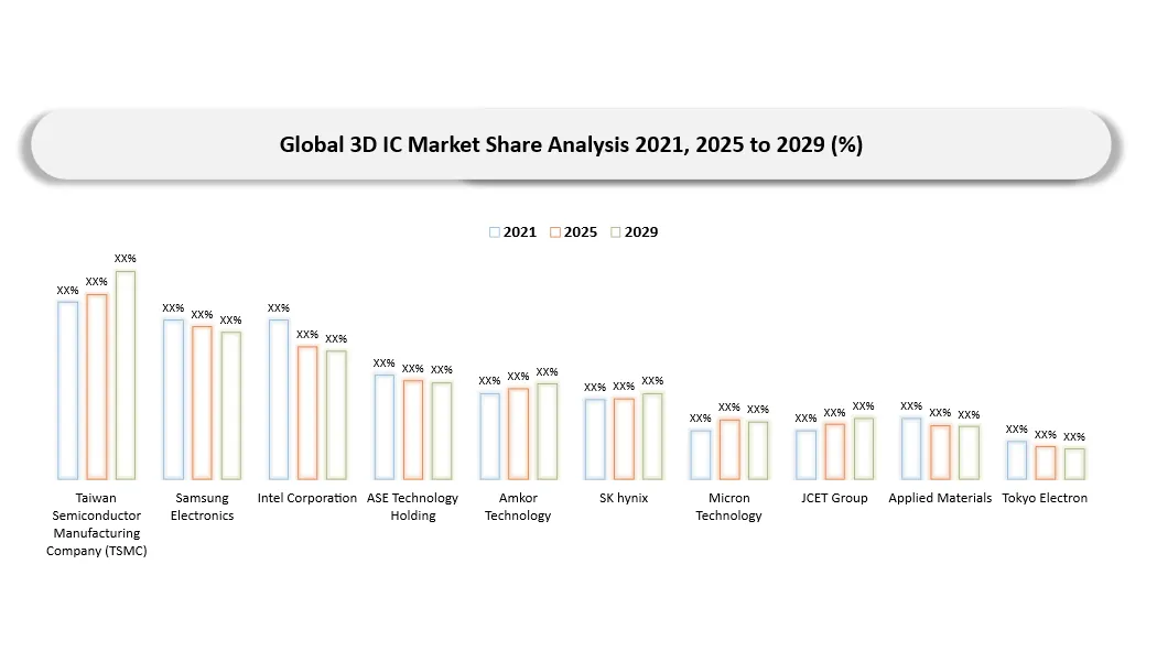
- TSMC leads foundry-integrated advanced packaging at scale, Samsung combines logic, memory and packaging, while ASE and Amkor remain leading outsourced packaging providers with expanding high-performance-compute exposure.
- Intel is developing foundry and advanced packaging platforms, while SK hynix and Micron are strategically important through stacked HBM and other 3D memory architectures.
- Market share can shift as new advanced processor programs qualify alternate packaging partners, and as hybrid bonding moves from pilot production into larger commercial volumes.
- Differentiation increasingly depends on package-level co-design, thermal engineering, known-good-die testing, bonding precision, substrate supply and the ability to scale yields quickly.
Market Ecosystem Table
| Value Chain Sector | Representative Companies | Role in 3D IC Market |
| EDA & 3D Design Enablement | Synopsys, Cadence, Siemens EDA, Ansys | 3D floorplanning, thermal/signoff, die-to-die verification and package co-design |
| Foundries & Integrated Packaging | TSMC, Samsung Foundry, Intel Foundry | Wafer fabrication plus CoWoS/SoIC, I-Cube/X-Cube, Foveros/EMIB-class integration |
| OSATs | ASE, Amkor, JCET, Powertech | Advanced assembly, wafer-level packaging, test and heterogeneous integration |
| Memory & HBM | SK hynix, Micron, Samsung Electronics | Vertically stacked DRAM and HBM for AI/HPC systems |
| Bonding / Assembly Equipment | Besi, ASMPT, EV Group, Tokyo Electron | Die attach, hybrid bonding, wafer bonding and assembly automation |
| Process Equipment | Applied Materials, Lam Research, Tokyo Electron | Deposition, etch, CMP and wafer processing for TSV and 3D integration |
| Inspection & Metrology | KLA, Onto Innovation, Camtek | Defect inspection, overlay and metrology for advanced packaging |
| Interposers / Substrates | Ibiden, Shinko, Unimicron, AT&S | Silicon/glass interposers, ABF substrates and redistribution structures |
| Materials | Entegris, DuPont, Resonac, Ajinomoto | Dielectrics, underfill, photoresists, bonding and substrate materials |
| Fabless / System Designers | NVIDIA, AMD, Broadcom, Apple, Qualcomm | Drive demand for chiplets, HBM and high-density 3D integration |
| Standards / Research | UCIe Consortium, JEDEC, imec, CEA-Leti | Chiplet interfaces, HBM standards and pre-competitive 3D integration R&D |
Public Company Q1-Q2 2026 Performance Comparison
| Public Company | Reporting Period | Q1-Q2 2026 Performance | Growth Indicator | Factors Driving 3D IC Growth |
| TSMC | Q2 2026 | US$40.20B net revenue; 67.7% gross margin | Revenue at top of guidance; strong AI/HPC demand | CoWoS, SoIC, HBM integration, chiplets and leading-edge logic |
| Amkor Technology | Q2 2026 | US$1.90B net sales; US$200M operating income | Net sales +26% YoY | Advanced packaging expansion, AI/HPC programs and U.S. capacity |
| Intel Corporation | Q1 2026 | US$13.6B total revenue; US$5.4B Intel Foundry revenue | Total +7% YoY; Foundry +16% YoY | Foveros/EMIB, wafer and advanced packaging demand, Penang assembly/test expansion |
| Micron Technology | Fiscal Q3 2026 | US$41.46B revenue; HBM4 in high-volume shipments for lead customer | Record quarterly revenue; HBM scaling | HBM3E/HBM4 stacking, advanced DRAM packaging and AI memory demand |
| Samsung Electronics | Q2 2026 guidance | Approx. KRW171T consolidated sales; KRW89.4T operating profit guidance | Strong rebound versus 2025 comparison | Foundry, HBM, memory stacking and integrated advanced packaging |
Key Companies
- Taiwan Semiconductor Manufacturing Company (TSMC)
- Samsung Electronics
- Intel Corporation
- ASE Technology Holding
- Amkor Technology
- SK hynix
- Micron Technology
- JCET Group
- Applied Materials
- Tokyo Electron
- KLA Corporation
- ASM International
- BE Semiconductor Industries (Besi)
- Synopsys
- Cadence Design Systems
Company Profiles
Taiwan Semiconductor Manufacturing Company (TSMC)
TSMC is the leading pure-play foundry and a major advanced packaging provider. Its 3DFabric portfolio, including CoWoS, InFO and SoIC, positions the company at the center of advanced processors, HBM integration, chiplets and high-performance 2.5D/3D systems.
Samsung Electronics
Samsung combines leading-edge foundry, memory and advanced packaging capabilities. Its strategic position spans HBM, wafer fabrication and 2.5D/3D integration, enabling vertically coordinated solutions for AI, mobile and high-performance computing.
Intel Corporation
Intel participates through Foveros 3D stacking, EMIB, advanced assembly and foundry services. Its roadmap emphasizes heterogeneous integration of compute tiles across process nodes, offering a route to modular high-performance systems.
ASE Technology Holding
ASE is one of the world’s largest OSAT providers, with capabilities in wafer-level packaging, fan-out, SiP, advanced substrate assembly and heterogeneous integration. Its scale and customer diversity make it a key 3D IC manufacturing partner.
Amkor Technology
Amkor provides advanced packaging and test services including 2.5D/3D, wafer-level and system-in-package solutions. Its expansion in Arizona and partnerships with leading ecosystem companies strengthen its position in AI/HPC packaging.
SK hynix
SK hynix is a leading HBM supplier and therefore a critical participant in 3D memory stacking. HBM3E and HBM4 roadmaps increase stack height, bandwidth and packaging complexity, deepening the company’s exposure to 3D integration.
Micron Technology
Micron supplies HBM and advanced DRAM products using 3D die stacking and sophisticated packaging. Its HBM4 and advanced stacked-memory roadmap links memory technology directly to next-generation advanced processor platforms.
Applied Materials
Applied Materials supplies deposition, etch, materials engineering and packaging equipment used across TSV formation, wafer thinning, bonding and advanced interconnect processes. It benefits as 3D integration adds more process steps per device.
BE Semiconductor Industries (Besi)
Besi is a leading semiconductor assembly equipment supplier with strong exposure to hybrid bonding and advanced die placement. Fine-pitch 3D integration creates a strategic growth opportunity as hybrid bonding moves into high-volume logic and memory applications.
Additional Company Coverage
Additional profiles and benchmarking include JCET Group, Tokyo Electron, KLA Corporation, ASM International, Synopsys and Cadence Design Systems, reflecting the broader equipment, test, design and outsourced packaging ecosystem supporting 3D IC commercialization.
3D IC Market Major Pain Points
- Multi-die yield can compound across stacked components, making known-good-die screening and process control essential.
- Thermal density increases as active dies are stacked vertically, limiting sustained performance without advanced heat-spreading and cooling.
- Hybrid bonding and fine-pitch TSV processes require extremely tight alignment, surface preparation and contamination control.
- Advanced packaging capacity remains concentrated among a limited number of foundries and OSATs.
- Large interposers and high-layer substrates can face warpage, supply and yield constraints.
- Testing internal die-to-die links and fault isolation becomes more complex in dense 3D systems.
- Long qualification cycles can slow adoption in automotive, aerospace and medical applications.
- Capital intensity is high across bonding, thinning, lithography, metrology and inspection equipment.
3D IC Market Recent Developments
- July 2026: TSMC reported Q2 2026 net revenue of US$40.20 billion and a 67.7% gross margin, reflecting exceptionally strong demand for leading-edge semiconductor manufacturing and advanced packaging-intensive AI products.
- July 2026: Amkor reported record Q2 2026 net sales of US$1.90 billion, up 26% year over year, and highlighted advanced packaging capacity expansion and AI/HPC customer programs.
- June 2026: TSMC and Amkor announced a long-term partnership to accelerate advanced packaging in the United States, strengthening the domestic ecosystem for high-performance heterogeneous integration.
- June 2026: Micron reported record fiscal Q3 2026 results and said HBM4 was in high-volume shipments for a lead customer, reinforcing strong demand for vertically stacked high-bandwidth memory.
- April 2026: Intel reported Q1 2026 revenue of US$13.6 billion and said the shift toward AI is increasing the need for its wafer and advanced packaging offerings; Intel Foundry revenue was US$5.4 billion.
- 2026: Semiconductor suppliers continued to expand advanced packaging, HBM, hybrid-bonding and chiplet capacity as advanced processors and data-center systems pushed package complexity higher.
Analyst View / Opinion on 3D IC Market
- 3D IC is moving from a specialized packaging technique into a core semiconductor scaling strategy. The most advanced processors increasingly depend on package-level integration to overcome reticle limits, memory-bandwidth bottlenecks and power constraints.
- Near-term leadership will be determined by HBM capacity, interposer and substrate availability, advanced packaging throughput and yield. Longer term, hybrid bonding and finer-pitch die-to-die interfaces will define competitiveness.
- AI and HPC will remain the strongest value driver, but automotive, photonics, imaging, RF and edge devices will broaden the market as vertical integration matures.
- Hybrid bonding should become increasingly important because it reduces interconnect pitch and parasitic power compared with micro-bump approaches, enabling denser logic-memory and logic-on-logic integration.
- Foundries and OSATs will continue to converge strategically, with customers seeking integrated wafer fabrication, packaging, test and co-design support.
- Equipment, materials, inspection and EDA suppliers can capture substantial value as 3D integration increases process complexity and requires new design methodologies.
3D IC Market Target Audience
| INDUSTRY | WHO SHOULD BUY THIS REPORT? | REASON TO BUY THIS REPORT |
|---|---|---|
| Foundries & OSATs | Advanced packaging, strategy and capacity-planning teams | Benchmark 3D integration technologies, customer demand and capacity expansion priorities. |
| Semiconductor Equipment | Product, sales and business-development teams | Assess hybrid bonding, TSV, thinning, inspection and metrology demand. |
| Memory & HBM Suppliers | Strategy, packaging and product teams | Quantify stacked-memory growth and integration requirements for AI/HPC. |
| Fabless & System Companies | Architecture, sourcing and package-design teams | Evaluate package platforms, suppliers, yield, cost and technology roadmaps. |
| Materials & Substrates | Commercial and R&D teams | Identify growth areas in interposers, substrates, bonding materials and thermal solutions. |
| Investors & Governments | Investment, policy and ecosystem-development teams | Track advanced packaging bottlenecks, regional capacity and strategic semiconductor dependencies. |
Why Choose DATAM?
- Data-driven insights combining foundry and OSAT disclosures, HBM roadmaps, advanced packaging capacity, semiconductor equipment trends and country-level electronics demand analysis.
- Post-purchase analyst consultations for market entry, competitive benchmarking, packaging strategy, equipment positioning and customer targeting.
- Annual report updates covering new 3D integration platforms, hybrid-bonding adoption, HBM generations, fab/OSAT expansion and market-share shifts.
- Specialized focus on semiconductor manufacturing hubs, public incentives and regional advanced packaging ecosystems.
- Actionable analysis connecting 3D IC demand with HBM, substrates, equipment, thermal management, yield and geopolitical constraints.
What DATAM Uniquely Provides
- Ten-year forecasts across integration type, interconnect technology, product/component, bonding method, application, end use, manufacturing model and material/integration platform.
- Architecture-level analysis linking TSVs, hybrid bonding, HBM, chiplets, interposers, substrates, test and thermal requirements.
- Competitive benchmarking of foundries, OSATs, IDMs, memory suppliers and advanced packaging equipment companies.
- Public-company 2026 performance comparison tied directly to 3D IC and advanced packaging growth drivers.
- Market ecosystem mapping from EDA and foundries through HBM, advanced packaging, equipment, materials, fabless customers and end-device OEMs.