photonic packaging market size
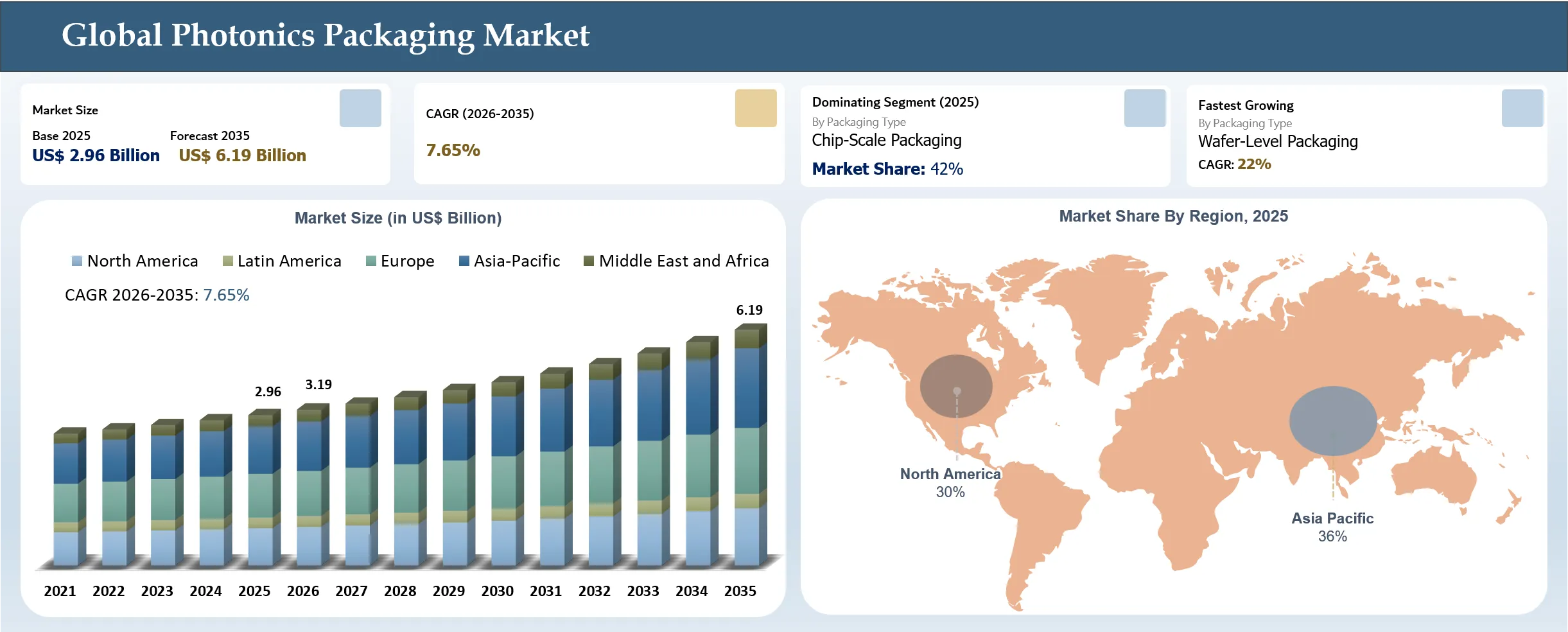
The global photonic packaging market reached US$ 2.96 billion in 2025 and is expected to reach US$ 6.19 billion by 2035, growing with a CAGR of 7.65% during the forecast period 2026-2033. The global photonic packaging market is expanding due to rapid advancements in optical communication technologies and increasing demand for high-speed, low-latency connectivity in AI, HPC, and data center networks. Companies and technology providers are actively responding with innovative solutions. For instance, in **2025, POET Technologies, a Canada‑based optical engine and photonic integration leader, partnered with South Korea’s Lessengers, an innovative optical solutions provider, to co‑develop a differentiated 800G DR8 transceiver for AI and hyperscale data center applications. This transceiver will integrate POET’s optical engines with Lessengers’ Direct Optical Wiring (DOW) technology to deliver a cost‑effective, high‑performance solution, with customer samples expected in the second half of 2025, demonstrating how strategic partnerships are accelerating the pace of advanced optical module development globally.
Key Takeaways
- The global photonics packaging market is projected to grow from US$ 2.96 billion in 2025 to US$ 6.19 billion by 2035, registering a 7.65% CAGR during 2026-2035.
- Chip-Scale Packaging dominates the market in 2025, accounting for 42% share, driven by high integration efficiency and compact device demand.
- Wafer-Level Packaging is the fastest-growing segment, expected to expand at a 22% CAGR, supported by increasing adoption of advanced miniaturized photonic devices.
- Asia Pacific leads the regional market with a 36% share in 2025, supported by strong semiconductor and photonics manufacturing capabilities.
- North America holds a significant 30% market share in 2025, driven by strong presence of hyperscale data centers, AI and cloud infrastructure investments, and technological advancements in silicon photonics and optical networking solutions.
Photonics Packaging Industry Trends and Strategic Insights
- Increasing adoption of AI infrastructure, cloud computing, and high-speed optical interconnects is accelerating demand for advanced photonics packaging solutions with higher bandwidth and lower latency performance.
- Rising transition toward chip-scale and wafer-level packaging technologies is enhancing miniaturization, thermal management, and integration efficiency across optical communication devices.
- Strong investments in silicon photonics and co-packaged optics are reshaping the competitive landscape, particularly in hyperscale data centers and next-generation telecom networks.
- Asia Pacific continues to strengthen its market leadership through expanding semiconductor fabrication and photonics manufacturing capabilities, while North America remains a key innovation hub for advanced optical technologies.
- Growing deployment of 5G, IoT, and high-performance computing applications is increasing the requirement for compact, energy-efficient, and high-density photonic packaging platforms.
- Strategic collaborations between semiconductor manufacturers, photonics companies, and packaging providers are accelerating innovation in heterogeneous integration and advanced optical packaging architectures.
Market Scope
| Metrics | Details | |
| 2025 Market Size | US$ 2.96 Billion | |
| 2035 Projected Market Size | US$ 6.19 Billion | |
| CAGR (2026-2035) | 7.65% | |
| Largest Market | Asia-Pacific | |
| Fastest Growing Market | Asia-Pacific | |
| By Packaging Type | Chip-Scale Packaging (CSP), Wafer-Level Packaging (WLP), Hybrid Packaging, Others | |
| By Component | Photonic Integrated Circuits (PICs), Lasers, Optical Modulators, Photodetectors, Optical Transceivers, Multiplexers, Others | |
| By Material | Ceramic, Metal, Polymer, Glass, Others | |
| By Application | Information, Communication, and Technology, Data Centers, Automotive, Consumer Electronics, Healthcare, Aerospace and Defense, Others | |
| By Region | North America | U.S., Canada, Mexico |
| Europe | Germany, UK, France, Spain, Italy, Poland | |
| Asia-Pacific | China, India, Japan, Australia, South Korea, Indonesia, Malaysia | |
| Latin America | Brazil, Argentina | |
| Middle East and Africa | UAE, Saudi Arabia, South Africa, Israel, Turkiye | |
| Report Insights Covered | Competitive Landscape Analysis, Company Profile Analysis, Market Size, Share, Growth | |
Why this report matters in 2026?
The Photonics Packaging Market report carries significant strategic relevance in 2026 as the industry experiences accelerated transformation driven by expanding AI infrastructure, hyperscale data centers, silicon photonics adoption, and next-generation optical communication networks. Increasing demand for high-speed data transmission, low-latency connectivity, and energy-efficient optical systems is intensifying the need for advanced photonics packaging technologies with enhanced integration, thermal management, and miniaturization capabilities. The market is also witnessing a strong transition toward chip-scale and wafer-level packaging architectures, positioning 2026 as a pivotal year for technology advancement, capacity expansion, and competitive differentiation across the value chain.
The report is particularly valuable for semiconductor manufacturers, photonics companies, OSAT providers, telecom equipment manufacturers, and optical component suppliers seeking to evaluate growth opportunities, technology adoption patterns, and regional expansion potential. Data center operators and AI infrastructure providers can leverage the study to assess future optical interconnect requirements and evolving packaging innovations supporting high-performance computing environments. Additionally, investors, private equity firms, and strategic stakeholders can utilize the report to identify high-growth segments, emerging investment opportunities, competitive benchmarking trends, and long-term market dynamics shaping the global photonics packaging industry.
Disruption Analysis
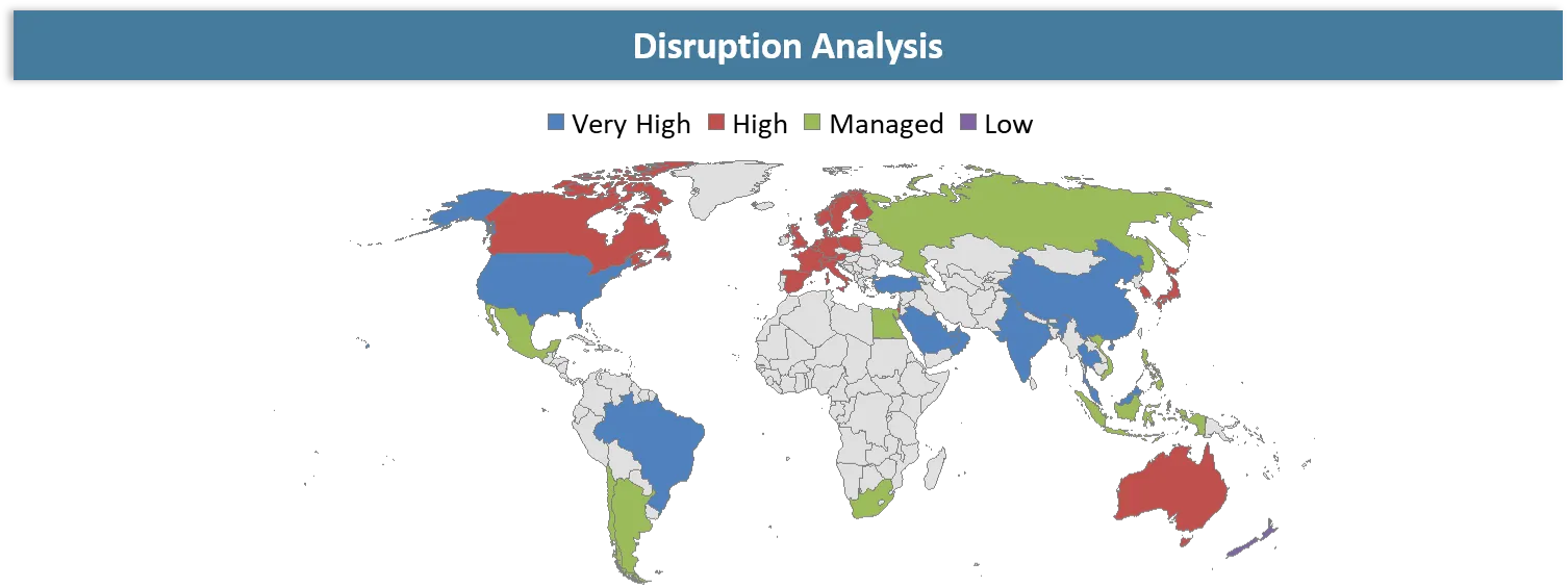
Shift from Electronic Packaging to Photonic-Electronic Co-Integration Reshaping Semiconductor System Design
One of the major disruptors of the photonics packaging industry is the transition from traditional packaging techniques to state-of-the-art photonic-electronic integrated systems. Conventional packaging techniques cannot handle the bandwidth, thermal performance, and signal integrity needs associated with AI applications. Photonics packaging can provide ultra-fast optical connectivity and highly efficient system integrations that will revolutionize semiconductor design. This trend disrupts the existing packaging companies and increases the need for specialized photonics foundries and assembly platforms.
A second major disruptor is the fast-emerging techniques of wafer-level packaging and hybrid packaging that facilitate the scalable manufacturing of photonic integrated circuits. This trend not only simplifies the manufacturing process but also ensures consistent performance in large-scale operations. The merging of silicon photonics and advanced packaging with automation is creating new paradigms for AI-based infrastructure solutions. Companies unable to integrate their systems into the emerging photonics packaging industry are likely to face severe competitive challenges.
BCG Matrix: Company Evaluation
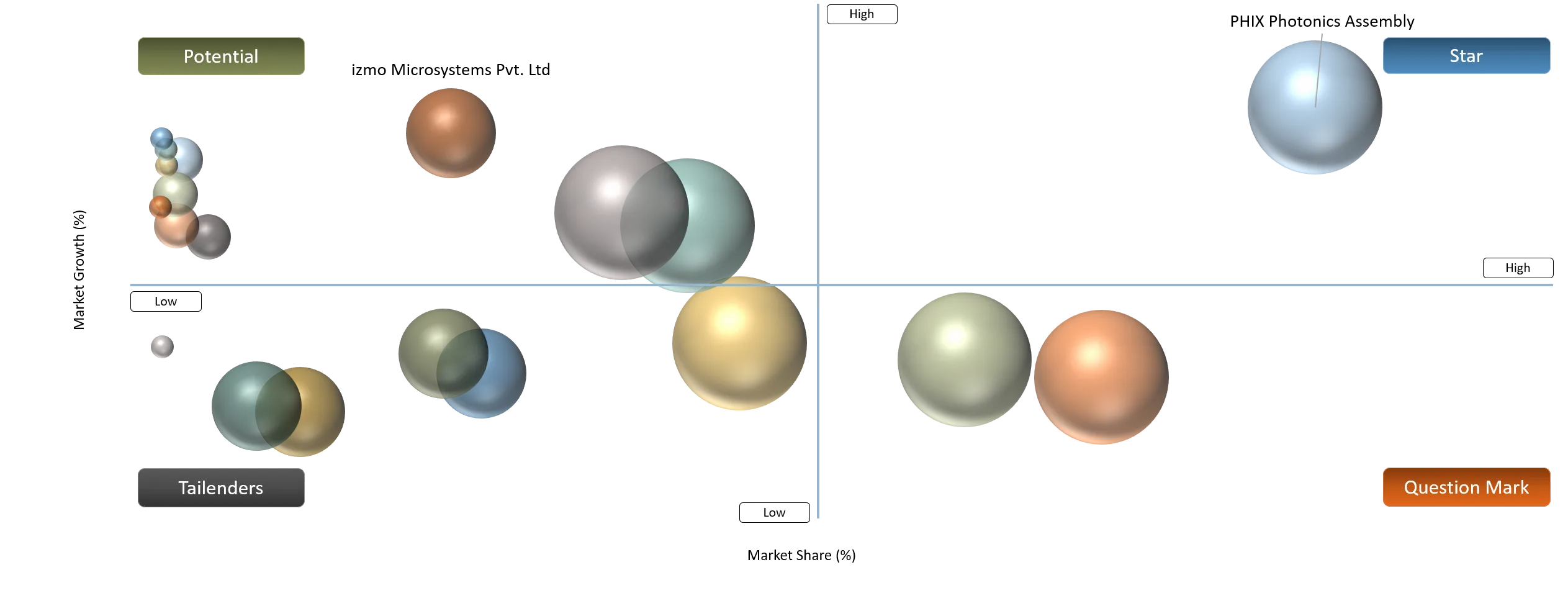
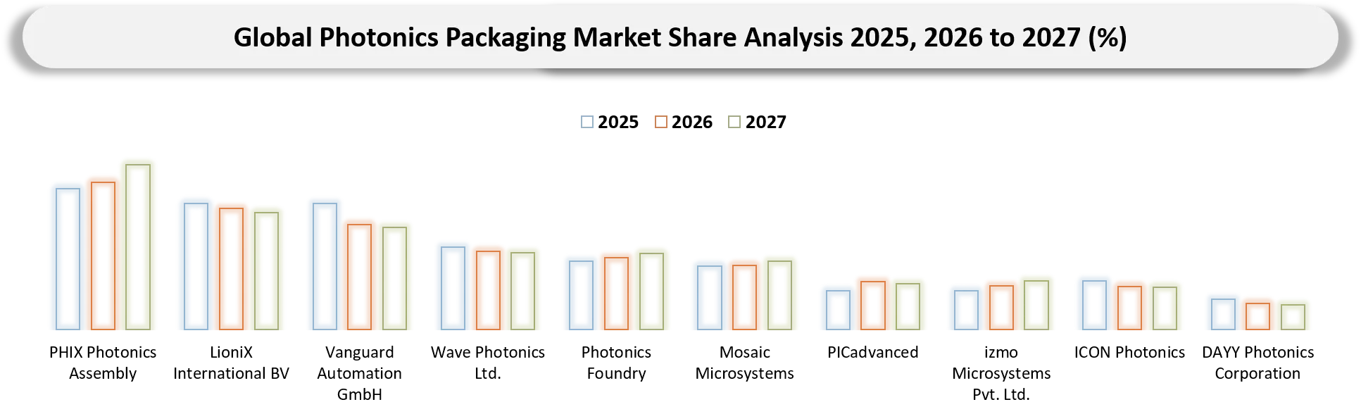
The market leaders in photonic packaging include companies like PHIX Photonics Assembly, LioniX International BV, and Vanguard Automation GmbH, which are identified as Stars due to their ability to cater to high demands for advanced photonic integration within AI data centers, optical interconnects, and future communications systems. These firms are boosted by robust photonics clusters in Europe, technical capabilities, and a rising preference for silicon photonics architectures. The firms' leadership is further enhanced by the rising demand for high-density and low-loss packaging solutions.
Firms like Wave Photonics Ltd., Photonics Foundry, Mosaic Microsystems, and PICadvanced have been placed in the category of Question Marks since these organizations operate in growing yet scaling photonic packaging and design ecosystems facing challenges in commercialization and scaling efforts. Early-stage firms like izmo Microsystems Pvt. Ltd., ICON Photonics, and DAYY Photonics Corporation are regarded as Potential due to their niche innovation capabilities but lack of global scale. On the other hand, the Tailenders consist of companies that provide early-stage or low-scale photonic packaging services.
Market Dynamics
Driver Impact Analysis
| Driver | Market Growth Impact (%) | Demand Concentration | Impacted Use Case | Strategic Impact |
Rising Adoption of AI Infrastructure and Hyperscale Data Centers | 8.5% | North America, China, South Korea, Taiwan | Optical interconnects, high-speed transceivers, co-packaged optics | Accelerates demand for high-bandwidth, low-latency, and energy-efficient photonics packaging solutions |
Expansion of Silicon Photonics Integration | 7.9% | North America, Europe, Asia-Pacific | Silicon photonics chips, optical engines, data communication modules | Strengthens commercialization of compact and highly integrated optical communication platforms |
Increasing Deployment of 5G and Next-Generation Telecom Networks | 7.2% | China, Japan, South Korea, North America | Fiber optic communication systems, telecom transceivers, RF photonics | Drives large-scale adoption of advanced optical packaging technologies for high-speed network infrastructure |
Growing Transition Toward Chip-Scale Packaging Technologies | 6.8% | Asia-Pacific, North America, Western Europe | Miniaturized optical devices, photonic integrated circuits (PICs) | Enhances device density, packaging efficiency, and thermal performance in compact photonic systems |
Rapid Advancement in Optical Communication Technologies
The continuous development of high-speed optical interconnects and integrated photonics is a key driver of the global photonic packaging and optical communication market. Modern data centers, AI workloads, and high-performance computing (HPC) systems demand ultra-high bandwidth, low-latency optical connectivity to support massive data flows between processors, memory, and storage. Companies are increasingly investing in photonic solutions that bypass traditional electrical interconnect limits, enabling faster, more efficient data transmission across large-scale computing infrastructures.
For instance, in 2025, Lightmatter, a California-based photonics company, unveiled the Passage M1000 Photonic Superchip, a 3D photonic interposer platform delivering a record-breaking 114 Tbps total optical bandwidth. The M1000 is designed to support massive die complexes and thousands of high-performance processors, leveraging dense waveguide networks and integrated fiber connectivity to overcome electrical I/O bottlenecks. Production readiness is supported through partnerships with GlobalFoundries and Amkor, demonstrating how next-generation photonic solutions are enabling high-speed AI and HPC interconnects, meeting the growing demand for efficient optical communication in data-intensive applications.
Restraint Impact Analysis
| Restraint | Drag on Market Growth (%) | Primary Impact Area | Impacted Use Case | Strategic Impact |
High Packaging and Manufacturing Costs | 5.2% | Advanced packaging scalability and production economics | Silicon photonics modules, co-packaged optics, optical transceivers | Limits large-scale commercialization and increases adoption barriers for cost-sensitive applications |
Complex Thermal Management Requirements | 4.8% | Device reliability and operational efficiency | AI data centers, high-performance computing systems, telecom infrastructure | Slows deployment of high-density photonic integrated systems due to overheating and performance degradation risks |
Lack of Standardization Across Photonics Packaging Platforms | 4.5% | Interoperability and supply chain integration | Multi-vendor optical communication systems, integrated photonic devices | Creates compatibility challenges and delays ecosystem-wide technology adoption |
Limited Availability of Advanced Packaging Materials | 4.3% | Material sourcing and manufacturing consistency | Wafer-level packaging, chip-scale photonics packaging | Increases supply chain vulnerabilities and production lead times |
Integration and Manufacturing Complexity Limiting Widespread Adoption
Despite rapid advancements in photonic packaging technologies like CSP and WLP, the market faces significant restraints due to complex integration requirements and high-precision manufacturing challenges. Aligning photonic components with electronic circuits at nanometer-scale tolerances, ensuring thermal stability, minimizing signal loss, and maintaining yield in high-volume production requires advanced equipment, specialized processes, and a highly skilled workforce. These constraints not only increase production costs but also slow the commercialization and scale-up of photonic modules for AI, HPC, and telecom applications, particularly for emerging companies lacking access to high-end fabrication facilities.
Segmentation Analysis
The global photonic packaging market is segmented based on packaging type, component, material, application, and region.
Rising Demand for Compact, High-Performance Chip-Scale Packaging (CSP) Drives the Photonic Packaging Market
Chip-Scale Packaging (CSP) is the dominant type with 42% share in the global photonic packaging market, as enterprises and hyperscalers seek compact, high-performance optical modules that deliver minimal footprint, short interconnect distances, and reliable high-bandwidth operation. CSP enables photonic modules to consistently deliver low-latency, high-throughput performance, which is why industries such as cloud computing, AI, telecommunications, and data centers rely heavily on CSP-based modules for optical interconnects and integrated photonic devices.
Photonic technology providers are actively extending CSP offerings to meet this demand. For instance, in 2024, Lightwave Logic, a Colorado-based photonic technology company, and Advanced Micro Foundry (AMF), a Singapore-based silicon photonics foundry, collaborated to develop advanced electro-optic polymer slot modulators on silicon photonics wafers, achieving record-low drive voltages and enabling 800 Gb/s and 1.6 Tb/s photonic transceivers for high-speed AI and data center applications. These advances illustrate how CSP continues to satisfy organizations’ needs for small form factor, high-performance, and reliable photonic interconnects.
Wafer-Level Packaging (WLP) Growth Driven by High-Throughput, Scalable Photonic Integration
The wafer-level packaging (WLP) segment, holding approximately 20% share, is the fastest-growing packaging type in the market, driven by its cost efficiency, scalability, and suitability for high-volume photonic device production. WLP enables multiple photonic devices to be packaged simultaneously at the wafer level, reducing manufacturing cycle times and maintaining precise alignment and thermal performance — critical for AI accelerators, high-performance computing (HPC), and large-scale optical networks.
For instance, in 2025, Advanced Semiconductor Engineering (ASE), a Taiwan-based advanced packaging provider, introduced the VIPack™ FOCoS-Bridge with Through Silicon Via (TSV), a wafer-level fan-out packaging innovation that reduces power loss, increases I/O density, and enhances thermal performance for AI and HPC workloads. Looking ahead to 2026, ASE is further evolving its FOCoS-Bridge platform with enhanced fan-out integration to support higher bandwidth and die-to-die interconnects for next-generation HPC and AI applications. These developments demonstrate how WLP is rapidly gaining adoption due to its scalability, efficiency, and ability to support next-generation high-performance photonic systems.
Geographical Penetration
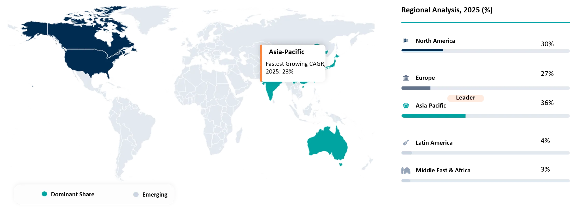
Rising Investments in Photonic Packaging in Asia-Pacific
Asia-Pacific is the dominating and fastest-growing region in the global photonic packaging market, holding the largest market 36% share in 2025. Governments and industry players across the region have been investing heavily in photonic integrated circuits (PICs) and high-performance photonic packaging to strengthen local technology ecosystems, support AI and telecom applications, and reduce reliance on foreign suppliers.
For instance, in 2025, the Singapore Semiconductor Industry Association (SSIA), in collaboration with the PhotonDelta Foundation, announced a strategic partnership to advance photonic integrated circuits (PICs). This initiative is aimed at fostering cross-border knowledge exchange, joint innovation, and local manufacturing capabilities for photonic devices and packaging solutions, positioning Singapore as a key hub for photonics development in Asia-Pacific.
China Photonic Packaging Market Outlook
China has emerged as a leading country in photonic chip production in the Asia-Pacific, driven by domestic R&D initiatives and national priorities around AI, quantum computing, and 6G technologies. Chinese institutions and startups have been investing heavily in next-generation photonic chips and integrated photonics, aiming for technological self-reliance and global competitiveness. For instance, in 2025, Shanghai Jiao Tong University’s Chip Hub for Integrated Photonics Xplore (CHIPX), a China‑based photonic research and manufacturing initiative, launched the country’s first thin‑film lithium niobate photonic chip production line—capable of producing ~12,000 6‑inch wafers annually with performance that surpasses previous global benchmarks in bandwidth and signal loss—aimed at accelerating domestic capabilities for AI, 6G, and quantum computing applications.
Japan Photonic Packaging Market Trends
Japan continues to advance its photonic and optical network ecosystem, driven by collaborations between major ICT vendors, carriers, and government‑aligned R&D initiatives aimed at next‑generation network infrastructure. For instance, in 2024, a consortium of Japanese companies, including NTT, KDDI, Fujitsu, NEC, and Rakuten Mobile, jointly launched a research program under Japan’s Beyond 5G/6G Innovative ICT Fund to develop cooperative All‑Photonics Network (APN) technologies that integrate photonic‑centric infrastructure for multi‑cloud and multi‑provider environments, advancing next‑generation telecom networks with improved capacity and resiliency.
Competitive Landscape
- The global photonic packaging market is characterized by a competitive landscape that includes both established and regional players.
- Key players include PHIX Photonics Assembly, LioniX International BV, izmo Microsystems Pvt. Ltd., Vanguard Automation GmbH, Photonics Foundry, ICON Photonics, DAYY Photonics Corporation, Wave Photonics Ltd., PICadvanced, Mosaic Microsystems
Key Developments
- In March 2026, NIST developed an advanced photonics packaging technology using hydroxide catalysis bonding (HCB) to enable photonic integrated circuits (PICs) to operate reliably under extreme conditions including radiation, cryogenic temperatures, and ultrahigh vacuum environments. The innovation strengthens deployment potential across quantum computing, aerospace, defense, and industrial sensing applications.
- In November 2025, Lightwave Logic, a Colorado-based technology platform company, launched a technical program with a second Fortune Global 500 partner to co-develop a custom variant of its Perkinamine electro-optic polymer material. The initiative targeted 400Gb/s Co-Packaged Optics (CPO) applications for AI networking, covering high-speed modulator simulation, product testing, packaging processes, and a Process Design Kit (PDK) for integration with silicon photonics foundry processes.
- In May 2025, SSIA and PhotonDelta formed a strategic partnership to strengthen global collaboration in photonic integrated circuits (PICs), focusing on photonic chip innovation, heterogeneous integration, testing, and advanced packaging to accelerate commercialization and ecosystem expansion.
- In June 2024, Wave Photonics, SENKO Advanced Components, and Alter Technology launched the QPICPAC packaging solution for quantum photonic integrated circuits (QPICs), enabling faster prototyping, reduced customization costs, and streamlined R&D development for quantum photonics applications.
- In May 2024, Vanguard Automation commissioned its SYMPHONY advanced photonic packaging platform at C2MI in Canada to support automated photonic integration, prototyping, and volume manufacturing applications. The deployment strengthens commercialization capabilities for telecom, datacom, optical computing, and quantum computing technologies through scalable and high-precision photonic packaging solutions.
Key Procurement Priorities and Buyer Evaluation Criteria
- Organizations investing in the global photonics packaging market are increasingly prioritizing vendors with capabilities in delivering scalable, high-precision, and thermally optimized packaging solutions that ensure long-term operational reliability, low signal loss, and advanced optical integration performance.
- Procurement strategies are being shaped by the accelerating adoption of silicon photonics, co-packaged optics, wafer-level packaging, and chip-scale integration technologies, alongside rising demand from AI infrastructure, hyperscale data centers, next-generation telecom networks, and high-performance computing environments.
- Semiconductor manufacturers, telecom equipment providers, hyperscale data center operators, and photonics device developers assess vendors based on optical alignment precision, thermal management efficiency, insertion loss performance, manufacturing scalability, packaging durability, and compatibility with advanced photonic integration architectures before finalizing technology partnerships and supplier selection decisions.
Why Choose DataM?
- Data-Driven Insights: Dive into detailed analyses with granular insights such as pricing, market shares and value chain evaluations, enriched by interviews with industry leaders and disruptors.
- Post-Purchase Support and Expert Analyst Consultations: As a valued client, gain direct access to our expert analysts for personalized advice and strategic guidance, tailored to your specific needs and challenges.
- White Papers and Case Studies: Benefit quarterly from our in-depth studies related to your purchased titles, tailored to refine your operational and marketing strategies for maximum impact.
- Annual Updates on Purchased Reports: As an existing customer, enjoy the privilege of annual updates to your reports, ensuring you stay abreast of the latest market insights and technological advancements. Terms and conditions apply.
- Specialized Focus on Emerging Markets: DataM differentiates itself by delivering in-depth, specialized insights specifically for emerging markets, rather than offering generalized geographic overviews. This approach equips our clients with a nuanced understanding and actionable intelligence that are essential for navigating and succeeding in high-growth regions.
- Value of DataM Reports: Our reports offer specialized insights tailored to the latest trends and specific business inquiries. This personalized approach provides a deeper, strategic perspective, ensuring you receive the precise information necessary to make informed decisions. These insights complement and go beyond what is typically available in generic databases.
Target Audience
- Manufacturers/ Buyers
- Industry Investors/Investment Bankers
- Research Professionals
- Emerging Companies