


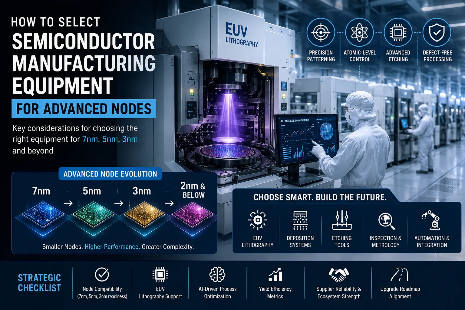
Selecting semiconductor manufacturing equipment for advanced nodes (7nm, 5nm, 3nm, and emerging 2nm technologies) requires evaluating precision capability, process compatibility, scalability, and cost efficiency. As AI, HBM, and advanced packaging technologies drive next-generation chip demand, equipment selection has become a strategic investment decision for fabs, OEMs, and investors. Key selection factors include lithography capability, process control accuracy, yield optimization, tool integration, and long-term upgrade compatibility.
Why Equipment Selection Matters in Advanced Semiconductor Nodes
The semiconductor industry is rapidly transitioning toward high-performance computing (HPC), AI accelerators, and advanced packaging architectures. As nodes shrink below 5nm, manufacturing complexity increases exponentially, making equipment selection a critical factor influencing yield, cost efficiency, and production scalability.
For semiconductor fabs, OSAT providers, and investors, choosing the right manufacturing equipment is no longer just a procurement decision it is a strategic technology investment decision.
What Are Advanced Nodes in Semiconductor Manufacturing?
Advanced nodes in semiconductor manufacturing refer to the most cutting-edge process technologies used to fabricate highly miniaturized and high-performance integrated circuits. These nodes represent the smallest transistor geometries currently in production and development, typically associated with leading-edge logic chips used in AI, high-performance computing (HPC), smartphones, and data center applications.
Common Advanced Node Classifications
Advanced semiconductor process nodes generally include:
- 7nm (nanometer class)
- 5nm
- 3nm
- 2nm and below (emerging next-generation nodes)
These “nm” values historically referred to transistor dimensions, but today they represent technology generations rather than exact physical measurements.
Why Advanced Nodes Are Technically Complex
As semiconductor nodes shrink, chip density increases significantly, but manufacturing becomes exponentially more complex. This requires extremely advanced fabrication capabilities across multiple process steps.
1. Extreme Precision Patterning
Advanced nodes require ultra-high-resolution patterning to define extremely small and densely packed transistor features.
- Utilizes EUV (Extreme Ultraviolet) lithography for sub-7nm nodes
- Requires nanometer-level alignment accuracy
- Supports highly complex multi-patterning techniques
Even minor deviations can impact chip performance and yield.
2. Atomic-Level Deposition Control
Material layers in advanced nodes are often only a few atoms thick.
- Requires atomic layer deposition (ALD) and precision chemical vapor deposition (CVD)
- Ensures uniform thickness across entire wafers
- Controls electrical properties at atomic scale
This level of precision is critical for transistor reliability and performance.
3. Advanced Etching Accuracy
Etching processes remove material to create circuit patterns with extreme precision.
- Uses highly selective plasma etching systems
- Requires near-perfect vertical and lateral control
- Must prevent damage to adjacent nanoscale structures
Etching precision directly impacts circuit integrity and yield.
4. Defect-Free Wafer Processing
At advanced nodes, even microscopic defects can render entire chips unusable.
- Requires ultra-clean fabrication environments (cleanrooms at near-zero contamination levels)
- Advanced inspection and metrology systems for defect detection
- Real-time process monitoring and AI-based defect prediction
Yield management becomes one of the most critical success factors in advanced semiconductor manufacturing.
Key Insight
Advanced nodes (7nm, 5nm, 3nm, and beyond) are not just smaller chips—they represent a fundamental shift in semiconductor manufacturing complexity, requiring integration of EUV lithography, atomic-scale material engineering, and AI-driven process control to achieve commercially viable production yields.
Key Factors for Selecting Semiconductor Manufacturing Equipment
1. Lithography Capability (Critical for Advanced Nodes)
Lithography is the most important determinant of node capability.
Selection criteria:
- EUV (Extreme Ultraviolet Lithography) compatibility
- Overlay accuracy and resolution control
- Throughput efficiency
- Defect minimization capability
EUV-ready equipment is essential for sub-7nm production.
2. Process Precision & Control Systems
Advanced nodes require atomic-level accuracy.
Key considerations:
- Process variation control (CD uniformity)
- Real-time monitoring systems
- AI-driven process correction
- Defect detection sensitivity
3. Equipment Compatibility with AI & HBM Manufacturing
Modern fabs must support:
- 3D stacking (HBM memory integration)
- Chiplet-based architectures
- Advanced packaging processes
- Heterogeneous integration
4. Yield Optimization Capability
Yield is a direct profitability driver.
Important factors:
- Wafer defect detection systems
- Predictive maintenance capabilities
- Machine learning-based process optimization
- High-volume production stability
5. Scalability & Future Node Upgrade Path
Equipment must support:
- Transition from 7nm → 5nm → 3nm
- Modular upgrade architecture
- Software-defined process tuning
- Long lifecycle usability
6. Cost of Ownership (TCO Analysis)
Beyond CAPEX, fabs must evaluate:
- Maintenance cost
- Energy consumption
- Downtime risk
- Spare parts availability
Semiconductor Equipment Categories for Advanced Nodes
Front-End Equipment
- Lithography systems
- Etching tools
- Deposition systems
- Cleaning systems
Back-End Equipment
- Assembly and packaging tools
- Testing systems
- Dicing and bonding equipment
AI, HBM & Advanced Packaging: The New Demand Drivers
The semiconductor equipment market is being reshaped by:
- Artificial Intelligence chips (GPU, TPU, AI accelerators)
- High Bandwidth Memory (HBM) demand
- 2.5D and 3D advanced packaging
- Chiplet architecture adoption
These technologies require:
- Higher precision equipment
- Advanced wafer bonding systems
- Thermal management solutions
- Ultra-clean manufacturing environments
Regional Equipment Selection Trends
The semiconductor manufacturing equipment landscape varies significantly across regions, driven by differences in industrial policy, technology leadership, supply chain ecosystems, and end-use demand. Understanding regional selection trends is critical for OEMs, fabs, and investors evaluating capital deployment and technology partnerships.
Asia-Pacific
Asia-Pacific remains the global center of semiconductor manufacturing capacity, accounting for the majority of advanced-node fabrication and packaging operations.
Key characteristics:
- Dominates global front-end wafer fabrication capacity
- Strong concentration of leading foundries and IDMs
- Aggressive adoption of EUV lithography and advanced deposition systems
- High demand for precision tools supporting 3nm, 5nm, and sub-5nm nodes
Equipment selection trends:
- Preference for high-throughput EUV lithography systems
- Strong demand for atomic-level deposition and etching equipment
- Rapid expansion of advanced packaging (2.5D/3D integration) tools
- Increased investment in automation and yield optimization systems
Strategic insight: Asia-Pacific continues to prioritize scale, efficiency, and cutting-edge node capability, making it the largest demand hub for advanced semiconductor equipment globally.
United States
The United States is experiencing a strong resurgence in semiconductor manufacturing driven by domestic chip production initiatives and AI infrastructure expansion.
Key characteristics:
- Significant investment in AI semiconductor fabs and HPC chip production
- Expansion of domestic manufacturing under strategic policy support
- Strong focus on reducing dependency on overseas supply chains
- High collaboration between fabless companies and equipment vendors
Equipment selection trends:
- High demand for AI-optimized manufacturing equipment
- Focus on tools enabling advanced logic chips and GPU/AI accelerators
- Investment in flexible, scalable fabrication systems
- Strong emphasis on automation, process intelligence, and smart fabs
Strategic insight: The U.S. market is shifting toward AI-driven semiconductor manufacturing ecosystems, with equipment selection focused on innovation and supply chain resilience.
Europe
Europe’s semiconductor equipment demand is more specialized, with a strong focus on automotive, industrial, and power semiconductor applications.
Key characteristics:
- Strong demand from automotive electronics (EVs, ADAS systems)
- Focus on power semiconductors, sensors, and industrial chips
- Policy-driven push for semiconductor self-sufficiency
- Emphasis on sustainability and energy efficiency
Equipment selection trends:
- Preference for power semiconductor fabrication equipment
- Growing demand for analog and mixed-signal production tools
- Investment in energy-efficient manufacturing systems
- Strong focus on quality, reliability, and long lifecycle equipment
Strategic insight: Europe is not competing on volume at advanced nodes but is building strength in specialized, high-reliability semiconductor segments.
Strategic Summary
Across regions, semiconductor manufacturing equipment selection is increasingly shaped by:
- Asia-Pacific → Scale + advanced node leadership
- United States → AI-driven semiconductor expansion
- Europe → Automotive + power semiconductor specialization
For investors and industry stakeholders, these regional differences highlight a clear shift toward diversified global semiconductor ecosystems, where equipment demand is becoming highly application-specific rather than uniform.
Key Challenges in Equipment Selection
- Extremely high capital investment requirements
- Rapid technology obsolescence
- Supply chain constraints for critical components
- Integration complexity across toolsets
Strategic Checklist for Buyers & Investors
Before selecting semiconductor manufacturing equipment, buyers, procurement heads, and investors must evaluate a combination of technology readiness, operational efficiency, and long-term scalability. Advanced semiconductor nodes (7nm, 5nm, 3nm, and beyond) require extremely precise manufacturing environments, where even minor equipment limitations can significantly impact yield, cost, and time-to-market.
Below is a detailed breakdown of the key evaluation criteria:
✔ Node Compatibility (7nm, 5nm, 3nm Readiness)
Equipment must be fully compatible with the target process node requirements. As semiconductor nodes shrink, the tolerance for variation becomes extremely narrow.
Key considerations include:
- Ability to support advanced node scaling (from 7nm to 3nm and below)
- Process stability at sub-nanometer precision levels
- Compatibility with next-generation transistor architectures (FinFET, GAA)
- Capability to handle complex multi-patterning processes
This ensures long-term usability and prevents early equipment obsolescence.
✔ EUV Lithography Support
Extreme Ultraviolet (EUV) lithography is a foundational requirement for advanced semiconductor manufacturing.
Evaluation factors include:
- EUV wavelength compatibility for sub-7nm fabrication
- Overlay accuracy and resolution precision
- Throughput efficiency for high-volume production
- Defect reduction capability in high-density chip designs
EUV readiness is a critical differentiator for advanced node production capability.
✔ AI-Driven Process Optimization Capability
Modern semiconductor manufacturing heavily relies on AI and machine learning for process control and efficiency improvements.
Key capabilities:
- Real-time defect detection using AI analytics
- Predictive maintenance to reduce downtime
- Adaptive process control for yield improvement
- Smart automation for wafer-level optimization
AI-enabled equipment significantly improves yield consistency and operational efficiency.
✔ Yield Efficiency Metrics
Yield is one of the most important financial and operational indicators in semiconductor manufacturing.
Important metrics to assess:
- Wafer defect density rates
- Process variation control (CD uniformity)
- First-pass yield performance
- Scrap rate reduction capability
Higher yield directly translates into improved profitability and reduced production costs.
✔ Supplier Reliability & Ecosystem Strength
The semiconductor equipment ecosystem is highly interconnected, making supplier reliability critical.
Key evaluation points:
- Proven track record in advanced node equipment supply
- Strength of global service and maintenance network
- Availability of spare parts and upgrade support
- Integration capability with other fab equipment vendors
A strong ecosystem reduces operational risk and improves production continuity.
✔ Upgrade Roadmap Alignment
Semiconductor technology evolves rapidly, making upgrade flexibility essential.
Key considerations:
- Modular hardware and software upgrade capabilities
- Compatibility with future node transitions (e.g., 5nm → 3nm → 2nm)
- Long-term vendor roadmap transparency
- Scalability for AI, HBM, and advanced packaging integration
Equipment with a clear upgrade path ensures long-term investment protection and reduces total cost of ownership.
Investor Takeaway
For investors and semiconductor manufacturers, selecting the right equipment is not only a technical decision but a strategic capital allocation choice. Equipment that aligns with advanced node requirements, AI-driven manufacturing, and long-term scalability will define competitive advantage in the next generation of semiconductor production.
Why This Matters for Investors
For investors and stakeholders, semiconductor equipment selection directly impacts:
- Fab profitability
- Technology competitiveness
- Long-term production scalability
- Market positioning in AI semiconductor supply chain
This makes equipment selection a key leading indicator of semiconductor industry growth cycles.
Conclusion
Selecting semiconductor manufacturing equipment for advanced nodes is a high-stakes strategic decision shaped by AI demand, HBM integration, and next-generation chip complexity. Companies that invest in scalable, EUV-ready, and AI-enabled equipment will be best positioned to lead the next wave of semiconductor innovation.